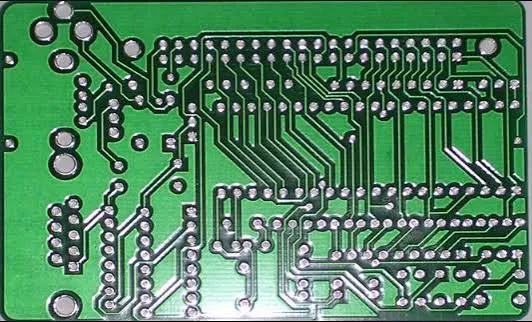
FPC trace to edge clearance is one of the most overlooked yet critical rules in flex PCB layout. Too little space and you risk trace damage during laser routing, exposed copper, and field failures. Getting the flex PCB edge spacing rule right saves yield and reliability headaches.
Recommended Safe Clearance Values for FPC Traces
For most commercial and industrial FPCs, maintain a minimum 0.15 mm clearance between the outer edge of any copper trace and the final laser-routed board outline. For higher reliability designs — medical, automotive, or dynamic bend applications — 0.20 mm to 0.30 mm is strongly preferred.
These numbers come from years of watching what actually works on the production floor. The extra margin accounts for real manufacturing variation rather than ideal CAD conditions.

Why 0.15 mm Is the Practical Minimum
Laser kerf width alone consumes 0.02–0.05 mm. Add positional tolerance of ±0.05 mm, coverlay registration error, and material movement during processing. Suddenly that "flush" or "near-flush" trace has no room left.
Below 0.10 mm the risk becomes unacceptable for most fabricators.
The Necessity of Inner Routing (Offset Traces)
Inner routing — deliberately pulling traces inward from the outline — is not just a nice-to-have. It is essential DFM practice for consistent quality.
When traces run parallel to the edge, any slight bow or tension release in the polyimide during laser cutting can cause the beam to nick the copper. Offsetting the traces creates a buffer zone that absorbs these variations.

When to Apply Aggressive Inner Routing
Use larger offsets near dynamic bend areas, connector interfaces, or stiffener boundaries. In high-layer-count flex or rigid-flex transitions, the accumulated stress makes proper edge spacing even more important.
Sometimes this means accepting a slightly larger overall panel size or rerouting a few signals. The trade-off is almost always worth it.
Tolerance Accumulation Considerations in FPC Edge Spacing
FPC trace to edge clearance must consider the full tolerance stack-up. Laser cutting tolerance, coverlay alignment (±0.075 mm typical), copper etching undercut, and panel handling all add together.
Material shrinkage after lamination or during thermal processes can shift features by another 0.05–0.1 mm. Ignoring this stack-up is where many otherwise solid designs fail DFM review.

Impact on Manufacturing Yield and Reliability
Insufficient clearance leads to higher scrap rates at routing, increased touch-up labor, and potential field returns from edge-related opens or shorts. Proper flex PCB edge spacing rule implementation consistently improves first-pass yield.
It also protects against long-term issues like copper oxidation at the cut edge and mechanical fatigue during repeated bending.
Practical Layout Guidelines for Designers
Set your design rules early: 0.20 mm minimum trace to outline for standard designs. Run DRC checks specifically for edge clearance. Review the gerber outline against all copper layers.
For critical signals, add extra margin or use guard traces. Document your clearance requirements in the fab notes so the CAM engineer understands your intent.
Communicating with Your Manufacturer
Share your intended clearance targets during the DFM stage. Experienced fabricators can suggest optimizations based on their specific laser equipment and process capabilities.
Sometimes a small design tweak — moving a via or adjusting a trace route — resolves an edge clearance issue without impacting electrical performance.
Key Engineering Takeaways on FPC Trace to Edge Clearance
The flex PCB edge spacing rule exists for good reason. Treating FPC trace to edge clearance as a non-negotiable DFM parameter rather than an afterthought prevents most laser-related defects and improves overall product robustness.
Next time you're tight on space, resist the urge to push traces all the way to the edge. A little breathing room goes a long way in manufacturing and in the field.
Proper clearance is not wasting space — it is engineering for manufacturability and long-term reliability.