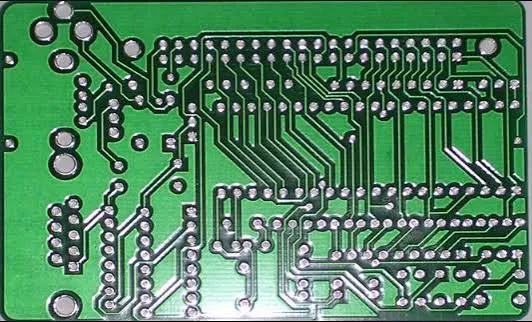
FPC adhesive overflow shows up more often than you'd expect when the tape is called out flush to the flex PCB outline. In DFM reviews, this is a classic tolerance stack-up issue that CAM engineers flag regularly. The tape ends up creeping past the final routed or punched edge, creating squeeze-out that can interfere with downstream processes or final assembly.
Most designers set the adhesive tape boundary exactly on the outline dimension thinking it will stay clean. Reality hits when you combine material movement, cutting registration, and the inherent variability of flex materials. This isn't a defect in every board, but it becomes a yield risk fast on tight-tolerance jobs.
How FPC Tape Tolerance Leads to Adhesive Overflow
FPC tape is often designed around the finished flexible PCB outline, but the tape position is not always identical to the final board geometry. Small variations can occur during tape cutting, lamination, bonding, and final FPC outline processing. When the tape is specified flush with the board edge, there is little room to absorb these variations.
Several tolerances can accumulate during manufacturing. The tape itself may shift slightly during placement, the flex PCB adhesive can move under pressure and heat, and the flexible substrate may change shape during lamination or subsequent processing. The final outline may also differ slightly from the intended CAD geometry.
When these variations occur in the same direction, the combined effect can push the adhesive layer beyond the FPC edge. This is why a tape dimension that appears correct in the design file can still result in visible adhesive overflow on the finished part.
For this reason, FPC tape should be treated as a manufacturing feature rather than simply a graphic layer. The tape boundary, board outline, bonding process, and expected production tolerance should be reviewed together during the design stage.

How FPC Tape Placement Is Affected by FPC Outline Processing
FPC tape placement is closely related to how the flexible PCB outline is manufactured. Laser cutting, die punching, routing, and other outline processes can produce different levels of dimensional variation and edge conditions.
The relationship becomes particularly important when the tape boundary is positioned very close to the final FPC edge. Even if the tape is accurately applied, the finished board outline may shift slightly relative to the tape.

Common FPC Tape Misalignment Patterns During Cutting
FPC tape misalignment does not always mean that the tape application process itself has failed. In many cases, the apparent misalignment is caused by the relationship between the tape reference position and the final board outline.
For example, if the tape is aligned to an internal feature during assembly while the final FPC outline is produced in a later process, a small difference between these references can become visible at the edge.
The effect is more noticeable when the tape extends directly to the nominal outline. A small change in the cutting position can expose the adhesive or leave the tape closer to the edge than intended.
The same principle applies to panelized production. Tape placement, panel registration, and individual board separation should be considered together when establishing the final tape boundary.
A practical approach is to define the tape position from a controlled reference feature and provide sufficient edge clearance rather than relying on the nominal FPC outline alone.
Why Flush FPC Tape Edges Create Reliability Risks
A flush FPC tape edge may look efficient because it maximizes the usable bonding area. However, it also removes the dimensional margin that can accommodate normal manufacturing variation.
When the adhesive reaches the finished FPC edge, even a small amount of movement can produce visible overflow. Depending on the application, excess adhesive can also affect nearby mechanical or electrical features.
For example, adhesive near a connector interface may interfere with insertion or assembly. Around exposed contact areas, insufficient tape clearance can create contamination or bonding concerns. In a foldable section, an abrupt tape boundary can also change the local stiffness of the flex.
The risk therefore extends beyond appearance. Tape placement can influence how the finished flexible PCB behaves during assembly and service.
A controlled setback between the tape edge and the finished FPC outline provides additional manufacturing margin. The appropriate clearance depends on the tape construction, substrate, manufacturing process, and application requirements, so it should be confirmed during the DFM review rather than treated as a universal value.

FPC Tape Design Rules to Prevent Misalignment and Overflow
A reliable FPC tape design should account for both the intended function of the adhesive and the manufacturing processes used to produce the flexible circuit.
Instead of defining the tape simply as an area that follows the board outline, the design should identify where adhesive is required, where it must be avoided, and how much clearance is needed around critical features.
FPC Tape Material and Process Considerations
The tape material can affect the final behavior of the flexible PCB. Adhesive type, tape thickness, bonding temperature, pressure, and dwell time can influence adhesive flow and the stability of the bonded structure.
During production, the tape may also be exposed to lamination or bonding pressure. If the adhesive becomes more flowable under the process conditions, material can move toward nearby edges or openings.
For this reason, tape selection should consider the complete assembly process rather than only the nominal bond strength.
The following factors should be reviewed during design and manufacturing evaluation:
- Tape and adhesive thickness
- Adhesive flow characteristics
- Bonding temperature and pressure
- Required bonding area
- Distance from the finished FPC edge
- Clearance from connector contacts and exposed copper
- Relationship with coverlay openings
- Stiffener and reinforcement boundaries
- Whether the flex area is static or dynamically bent
For dynamic applications, the tape boundary also deserves special attention. A tape layer can locally increase stiffness, creating a transition between the reinforced and flexible portions of the circuit. The transition should be positioned carefully to avoid concentrating mechanical stress in a bend zone.
How to Specify FPC Tape Clearance in Manufacturing Drawings
The tape area should be clearly defined in the fabrication or assembly documentation instead of relying only on the FPC outline shown in the PCB artwork.
A complete specification can identify the tape type, thickness, bonding area, tape boundary, required edge clearance, and restricted regions. This gives the manufacturer a clear reference for CAM and DFM review.
Critical areas should receive particular attention. Connector contacts, exposed pads, test points, coverlay openings, stiffeners, and fold zones may require different tape boundaries depending on the function of the assembly.
If adhesive must not extend into a specific area, that restriction should be explicitly stated in the drawing or manufacturing notes.
This is especially useful when the FPC tape and final board outline are created at different manufacturing stages. A clearly defined tape boundary helps the manufacturer evaluate registration and tolerance relationships before production.
For the complex FPCB assembly, the tape specification should also be reviewed against the complete stackup. Tape, coverlay, copper, stiffener, and other reinforcement layers can all affect the finished thickness and mechanical behavior of the flex.
Conclusion: Designing FPC Tape for Reliable Manufacturing
FPC tape is a relatively small part of a flexible circuit assembly, but its placement can have a significant effect on manufacturing consistency and assembly reliability.
When the tape edge is designed flush with the finished FPC outline, normal variation in tape placement, adhesive movement, lamination, and final cutting can leave little room for error. The result may be adhesive overflow, visible misalignment, or interference with nearby features.
A more reliable approach is to treat FPC tape as a controlled manufacturing feature. Define the tape boundary clearly, allow appropriate clearance from the finished FPC edge, consider adhesive behavior during bonding, and check the tape against the FPC connector, coverlay openings, stiffeners, and flexible regions.
For production designs, early DFM review can help identify these conflicts before fabrication begins. By considering FPC tape placement together with the complete flex PCB structure and manufacturing process, designers can reduce avoidable edge problems while improving consistency in production.
FAQ
Q1: What materials are commonly used for FPC tape?
A1: FPC tape can use different carrier and adhesive constructions depending on the application. Common options include polyimide-based films, polyester films, acrylic adhesive systems, and other engineered adhesive materials. The appropriate construction depends on temperature exposure, flexibility, bonding requirements, and the surfaces being joined.
Q2: What is the difference between FPC tape and ordinary adhesive tape?
A2: FPC tape is selected for the mechanical, thermal, and assembly requirements of flexible circuits. Compared with general-purpose adhesive tape, it may need better dimensional stability, controlled thickness, stronger bonding performance, or compatibility with the materials used in an FPC assembly.
Q3: Can FPC tape withstand high temperatures?
A3: Some FPC tapes are designed for elevated-temperature applications, but temperature resistance varies significantly by tape construction and adhesive system. The relevant specification should consider both short-term processing temperatures and the long-term operating temperature of the finished assembly.
Q4: Is FPC tape electrically conductive?
A4: Most FPC bonding tapes are electrically insulating. Conductive adhesive tapes are also available for applications that require electrical or grounding connections. The choice should be based on the required electrical function rather than assuming that all FPC tape provides conductivity.
Q5: Can FPC tape be used with polyimide flexible PCBs?
A5: Yes. FPC tape can be used with polyimide flexible circuits when the adhesive and tape construction are compatible with the polyimide surface and the intended assembly process. Surface condition, bonding temperature, required flexibility, and service environment should be considered when selecting the tape.
Q6: What factors should be considered when selecting FPC tape?
A6: Important factors include adhesive type, carrier material, total thickness, bond strength, flexibility, temperature resistance, environmental exposure, and compatibility with the materials being bonded. The expected assembly method and service conditions should also be considered before selecting a tape specification.
Q7: Can FPC tape be removed after assembly?
A7: Some adhesive tapes are designed for permanent bonding, while others offer removable or repositionable characteristics. Whether an FPC tape can be removed depends on the adhesive system, bonding conditions, substrate, and required removal method. For production assemblies, the manufacturer's removal and rework requirements should be confirmed before material selection.