FPC Process Edge vs Customer Outline: Which Panel Strategy Delivers Better Yield in Production
In flexible PCB manufacturing, the decision to add process edges (manufacturing borders) or rely purely on the customer's final outline has a direct impact on handling damage, panel utilization, and overall yield. From the factory perspective, adding controlled process edges is usually the safer choice for most production runs, while tight customer outline designs suit only specific low-risk, prototype, or high-volume optimized cases.
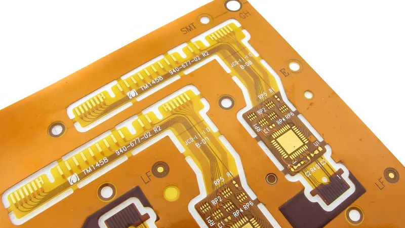
FPC Process Edge vs Customer Outline: Key Manufacturing Trade-offs
| Factor | With Process Edge | Customer Outline Only |
|---|---|---|
| Handling Protection | Excellent (reduces edge damage) | High risk during processing |
| Panel Utilization / Material Efficiency | Moderate (more scrap) | Higher (tighter nesting) |
| Production Yield | Higher overall | Lower due to handling issues |
| Cost per Panel | Higher material usage | Lower raw material cost |
| Lead Time Impact | Standard | Potentially faster setup |
| Suitable for High Volume | Preferred | Only with optimized design |
| Routing / Depanelization | More controlled | More challenging |
Decision Matrix: When to Add Process Edges vs Use Customer Outline
| If your priority is... | Better Choice | Why from Production View |
|---|---|---|
| Highest possible yield & reliability | Process Edge | Protects delicate flex edges during lamination, drilling, and plating |
| Maximum material cost saving | Customer Outline | Better panel utilization reduces base material cost |
| Prototype or quick-turn | Customer Outline | Simpler layout, faster CAM if no added features needed |
| Complex multi-up arrays | Process Edge | Better stability during processing of thin flex materials |
| High-volume mass production | Process Edge (recommended) | Consistent quality outweighs marginal material savings |
| Ultra-thin or special materials | Process Edge | Critical for preventing tearing and deformation |
Yield and Risk Comparison Between Process Edge and Customer Outline Strategies
During daily production of flexible circuits, we see clear differences in defect rates. Adding process edges provides a handling buffer that significantly reduces edge chipping, tearing, and delamination — common issues when relying solely on the customer's final outline. In practice, this can improve overall panel yield by 8-20% depending on design complexity and material thickness.
Customer outline-only panels maximize copper and polyimide utilization but expose the actual part edges to mechanical stress throughout the entire fabrication process, including layup, pressing, drilling, and plating. This risk becomes especially noticeable with thinner flex materials (under 50μm) or designs with fine features near the perimeter.
Manufacturing Considerations: Process Stability and Panel Strategy
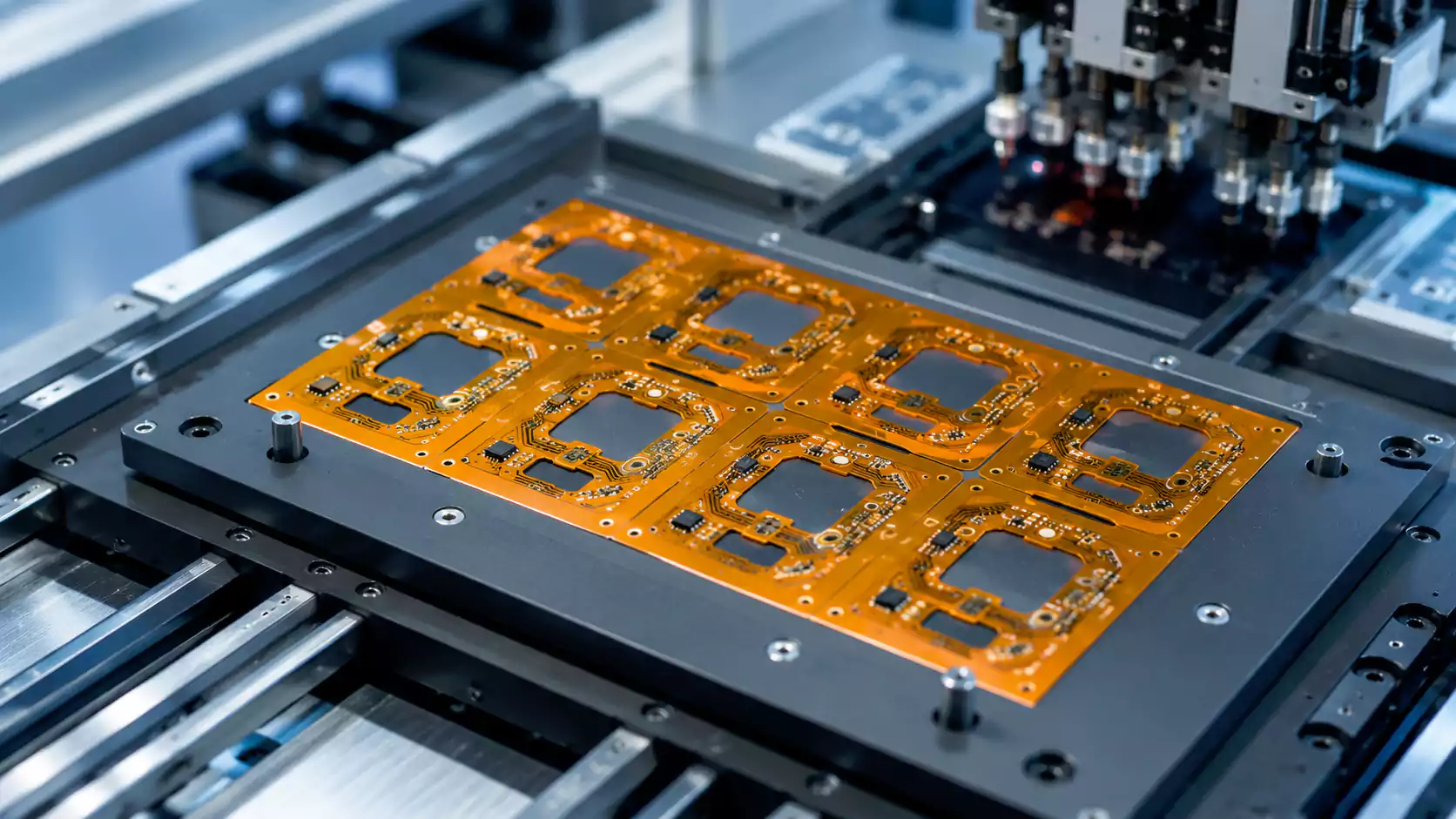
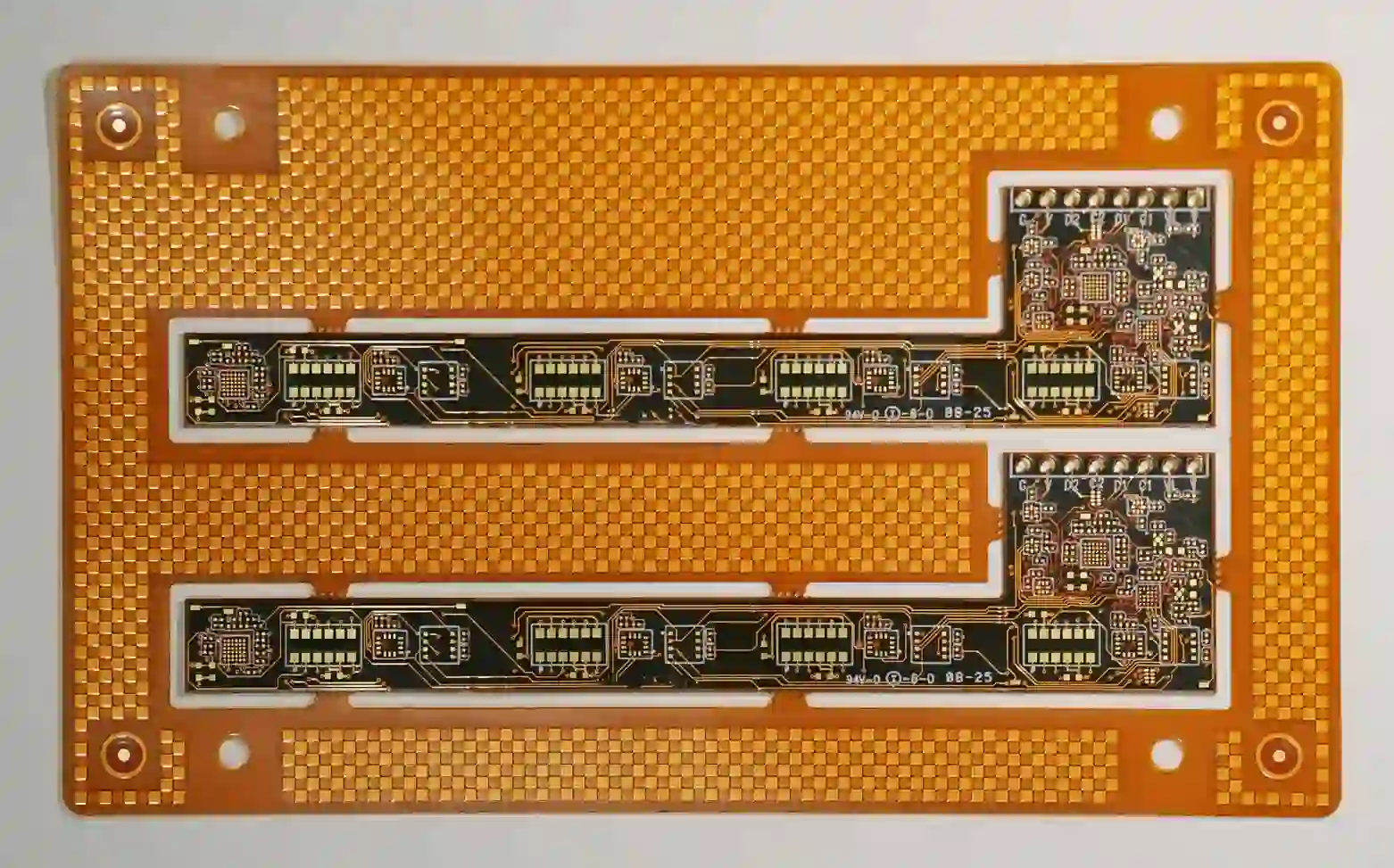
In CAM engineering for FPC, adding process edges allows us to incorporate registration holes, fiducials, and handling tabs in non-critical areas. This improves alignment accuracy and reduces scrap from misregistration. Pure customer outline designs often force us to use the part itself for tooling features, increasing the chance of damaging functional areas.
Routing and depanelization are also more predictable with added edges. We can use standard breakaway tabs or scoring that keeps the final part clean. With tight outlines, every handling step carries higher risk of cosmetic or functional defects that may only appear during final inspection or assembly.
Factory Perspective on FPC Process Edge vs Customer Outline
Most PCB manufacturers prefer adding process edges for the majority of flexible PCB orders because it stabilizes the production process and delivers more consistent quality. During DFM review, we evaluate panel fit, material thickness, and feature density to decide the optimal border width — typically 5-10mm depending on panel size.
For very high-volume runs with mature designs, we can work with optimized customer outlines if the customer accepts the associated yield risk and potential for higher unit pricing due to increased scrap. In practice, the total cost benefit of tight nesting is often smaller than expected once rework and lower yield are factored in.
Which Panel Strategy Should You Choose for Your FPC?
Add Process Edges if you:
- Require high reliability and consistent yield
- Use thin or delicate flex materials
- Have complex designs with fine features near edges
- Are running medium to high volume production
- Want to minimize assembly line defects
Rely on Customer Outline if you:
- Need maximum material efficiency for cost reduction
- Are producing simple prototypes or low-volume runs
- Have a very mature design with proven handling processes
- Accept slightly higher per-unit risk for lower base price
Frequently Asked Questions
Q1: How much does adding process edges increase the cost of FPC production?
A1: It typically adds 5-15% to material usage depending on panel layout. However, the improved yield often offsets this through fewer rejected panels.
Q2: Can process edges be removed cleanly from the final FPC parts?
A2: Yes. Factories use precise routing or laser cutting with breakaway tabs to ensure clean separation without damaging the customer outline.
Q3: When is customer outline only acceptable for flexible PCBs?
A3: It works best for simple, rigid-flex transition areas or very high-volume standardized designs where handling procedures are tightly controlled.
Q4: Does adding process edges affect lead time for FPC orders?
A4: Minimal impact in most cases. The extra CAM work is small compared to the benefits in process stability.
Q5: What is the typical width for recommended process edges on flex panels?
A5: Usually 5-10mm, adjusted based on panel size, material thickness, and specific process requirements.