Top 3 DRC Details Causing Real PCB Failures Video
What This Video Covers
This video breaks down the top three DRC details most responsible for real-world PCB production failures: trace and pad spacing, solder mask bridge width, and power/ground line width, spacing, and via sizing. It explains how designs that appear perfect on screen can still fail once manufacturing and assembly tolerances are applied, resulting in shorts, solder bridges, voltage drop, and noise.
The content emphasizes that boards which barely pass DRC are usually the first to encounter problems on the production line. Viewers learn practical ways to strengthen these specific checks for higher reliability. For fast validation of your designs, start with our PCB prototype service or request full production support through PCB Assembly. High-volume projects can also explore PCB mass production with built-in DRC review.
Key Highlights
- Insufficient trace/pad spacing and narrow solder mask bridges are leading causes of shorts and solder bridges in production
- Ignoring power and ground DRC rules (width, spacing, via size) often results in voltage drop and noise issues
- Designs that barely pass DRC are the most likely to fail once real manufacturing tolerances are applied
Understanding DRC in Real Manufacturing Contexts
Design Rule Checks (DRC) serve as the first line of defense in PCB layout, but many engineers treat them as a simple pass/fail checkbox rather than a comprehensive manufacturability evaluation. In actual production environments, especially for multilayer FR-4, HDI, and high-density boards, even minor DRC violations compound with etching tolerances, registration shifts, solder mask application variations, and assembly placement inaccuracies.
Factories routinely observe that boards passing DRC with minimal margins frequently experience yield loss during lamination, plating, or reflow. Understanding the interaction between design intent and process capabilities is essential for reducing Engineering Questions (EQs) and improving overall reliability.
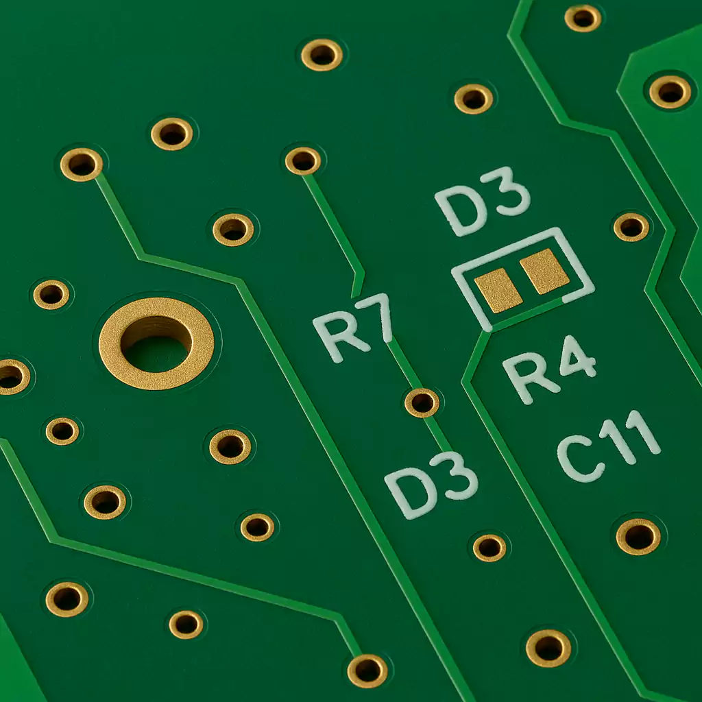
Critical Trace and Pad Spacing Rules
Trace-to-trace, trace-to-pad, and via-to-trace clearances represent some of the most frequent sources of shorts in production. When these gaps fall below recommended manufacturing minimums—typically 0.15–0.20 mm for standard processes on 1 oz copper—etching undercut and plating variations can eliminate the intended isolation. Fine-pitch components and dense routing further amplify the risk.
In practice, high-density designs that rely on the absolute minimum clearance often require additional teardrops or annular ring adjustments. Without these reinforcements, minor misregistration during drilling or imaging leads to breakout or bridging. Engineers should adopt conservative spacing guidelines based on the chosen stackup and copper weight rather than relying solely on EDA tool defaults.
Solder Mask Bridge Width Challenges
Solder mask bridges narrower than 0.10–0.15 mm (depending on the process) frequently fail during application or reflow. Thin bridges tear easily, lift, or provide incomplete coverage, allowing solder to flow between adjacent pads and create shorts—particularly problematic for QFN, BGA, and fine-pitch SMD packages.
Production data consistently shows higher defect rates when bridge widths approach process limits. Recommended practice includes verifying minimum bridge requirements with the fabricator early and considering mask-defined pads or increased clearance for high-reliability applications.
Power and Ground Plane Design Essentials
Power and ground networks demand stricter DRC adherence than most signal traces due to current-carrying requirements. Inadequate trace width causes voltage drop and localized heating, while insufficient via sizing or quantity leads to high inductance, noise coupling, and EMI issues. In multilayer boards, poor plane stitching exacerbates these problems during high-speed or high-current operation.
Real manufacturing scenarios often reveal that marginal power/ground vias suffer from plating voids or weak connections after thermal stress, compromising long-term reliability. Proper via arrays, copper pour optimization, and impedance-aware stackups help maintain signal integrity and thermal performance.
How Manufacturing Tolerances Expose Weak DRC Checks
| Parameter | Typical DRC Minimum | Recommended Production Margin | Common Failure Mode |
|---|---|---|---|
| Trace/Pad Spacing | 0.15 mm | 0.20–0.25 mm | Etch undercut → shorts |
| Solder Mask Bridge | 0.10 mm | 0.15–0.20 mm | Bridge tear → solder bridging |
| Power Trace Width | Per current calc | +20–30% margin | Voltage drop & overheating |
| Ground Via Size/Count | 0.30 mm | Multiple stitched vias | High inductance & noise |
This table highlights how minimal DRC compliance translates to production risk. Applying appropriate margins during layout significantly reduces EQ frequency and improves first-pass yield.
Practical DFM Strategies for Robust PCB Designs
Effective DFM begins with early fabricator consultation and stackup-specific rule sets. Incorporate annular ring reinforcements, teardrops on vias, and controlled impedance considerations where required. Regular design reviews focusing on the three critical DRC areas—spacing, solder mask, and power/ground—prevent most common failures.
For complex projects, prototype runs with full CAM review provide valuable feedback before committing to mass production. Documenting lessons from previous EQ cases helps teams build institutional knowledge and refine future layouts systematically.
FAQ
Q1: What are the most common spacing-related DRC violations that cause PCB shorts?
A1: The most frequent spacing violations include insufficient trace-to-trace, trace-to-pad, and via-to-trace clearances. When manufacturing and assembly tolerances stack up, these marginal gaps result in unintended shorts, especially on high-density or fine-pitch boards.
Q2: How narrow can solder mask bridges be before they cause assembly failures?
A2: Solder mask bridges narrower than the manufacturer's minimum (typically 0.1 mm or less) are prone to tearing, incomplete coverage, or lifting during reflow. This commonly leads to solder bridging between adjacent pads, particularly with fine-pitch components or BGA packages.
Q3: Why do power and ground DRC rules matter more than signal traces in high-current designs?
A3: Power and ground traces carry significantly higher current, so inadequate width causes voltage drop and overheating, while insufficient spacing or via sizing leads to noise, EMI, and long-term reliability issues. These rules are critical because even small violations can compromise the entire board's performance, unlike most signal traces.
Q4: How can engineers quickly validate DRC settings before sending files for PCB prototyping?
A4: Run DRC with fabricator-specific rule files, review spacing and solder mask in 3D views, and request a preliminary CAM check. Focus on the top three risk areas and apply conservative margins for copper weight and layer count to minimize surprises during production.
Q5: What role do manufacturing tolerances play in DRC-related failures?
A5: Even perfect layouts encounter etching tolerances (±0.02–0.05 mm), registration shifts, and solder mask alignment variations. Designs operating at absolute minimums frequently fail when these real-world factors accumulate, underscoring the need for production-aware DRC practices.
Let's talk about the top three DRC details that cause the most real-world failures:spacing, solder mask, and power or ground.
You might route traces and pads too close,leave very narrow solder mask bridges,and ignore power or ground DRC rules like line width, spacing, and via sizing.
On screen, everything looks fine.
But once manufacturing and assembly tolerances stack up,shorts, solder bridges, voltage drop, and noise start to appear.
Check spacing, solder mask, and power or ground together.
If a design barely passes DRC,it's usually the first one to fail in production.
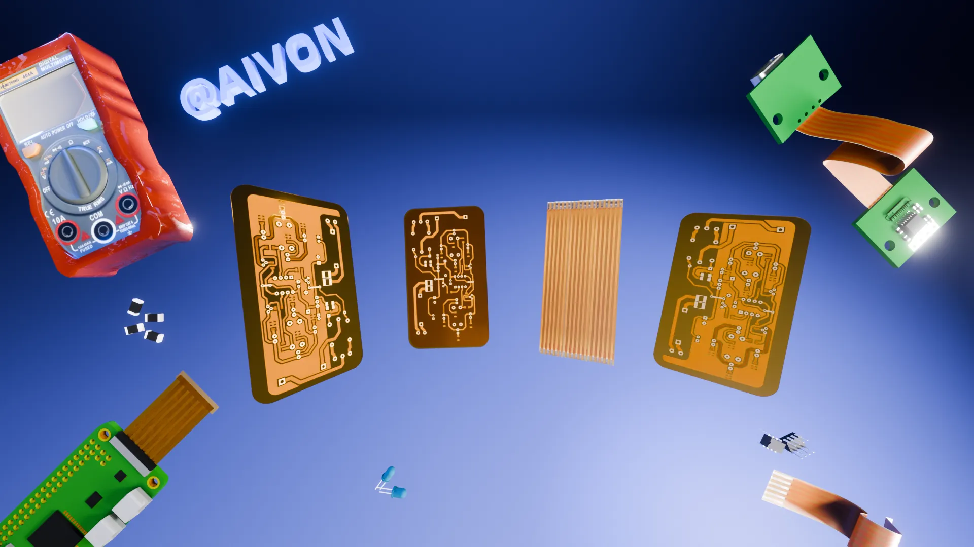
This is AIVON, Save this for your next design review.