 00:42
00:42
PCB Grounding
PCB grounding is a fundamental aspect of printed circuit board design that ensures reliable performance, minimizes electromagnetic interference, and enhances overall system stability. In electronics engineering, effective grounding techniques provide a low-impedance path for current return, preventing issues such as signal distortion, noise coupling, and potential safety hazards in high-frequency or power-intensive applications. Whether you are designing consumer gadgets, automotive systems, or industrial controls, understanding PCB grounding principles can significantly improve circuit integrity and compliance with standards like EMC regulations. This tag page compiles articles and resources focused on PCB grounding strategies, including single-point versus multi-point grounding, the role of ground planes in multilayer boards, and methods to mitigate ground loops. For engineers and hobbyists searching for practical guidance, these materials offer actionable insights into selecting appropriate grounding topologies based on circuit requirements, such as analog-digital separation or high-speed signal routing. Best practices highlighted here include using vias for efficient ground connections, incorporating decoupling capacitors, and simulating ground paths with tools like SPICE to predict and resolve potential problems before prototyping. By applying these techniques, you can achieve better noise immunity in mixed-signal designs and reduce the risk of failures in real-world deployments. For instance, proper PCB grounding is crucial in RF applications to maintain signal fidelity and in power electronics to handle transient currents safely. If you are troubleshooting persistent EMI issues or optimizing a new layout, the articles linked under this tag provide step-by-step tutorials and case studies to refine your approach. Diving into these resources will equip you with the knowledge to implement robust grounding solutions tailored to your projects.
Video Guide
-
00:42
Technical Articles
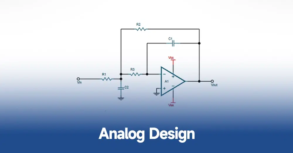
The Nine Stages of Analog Circuit Design
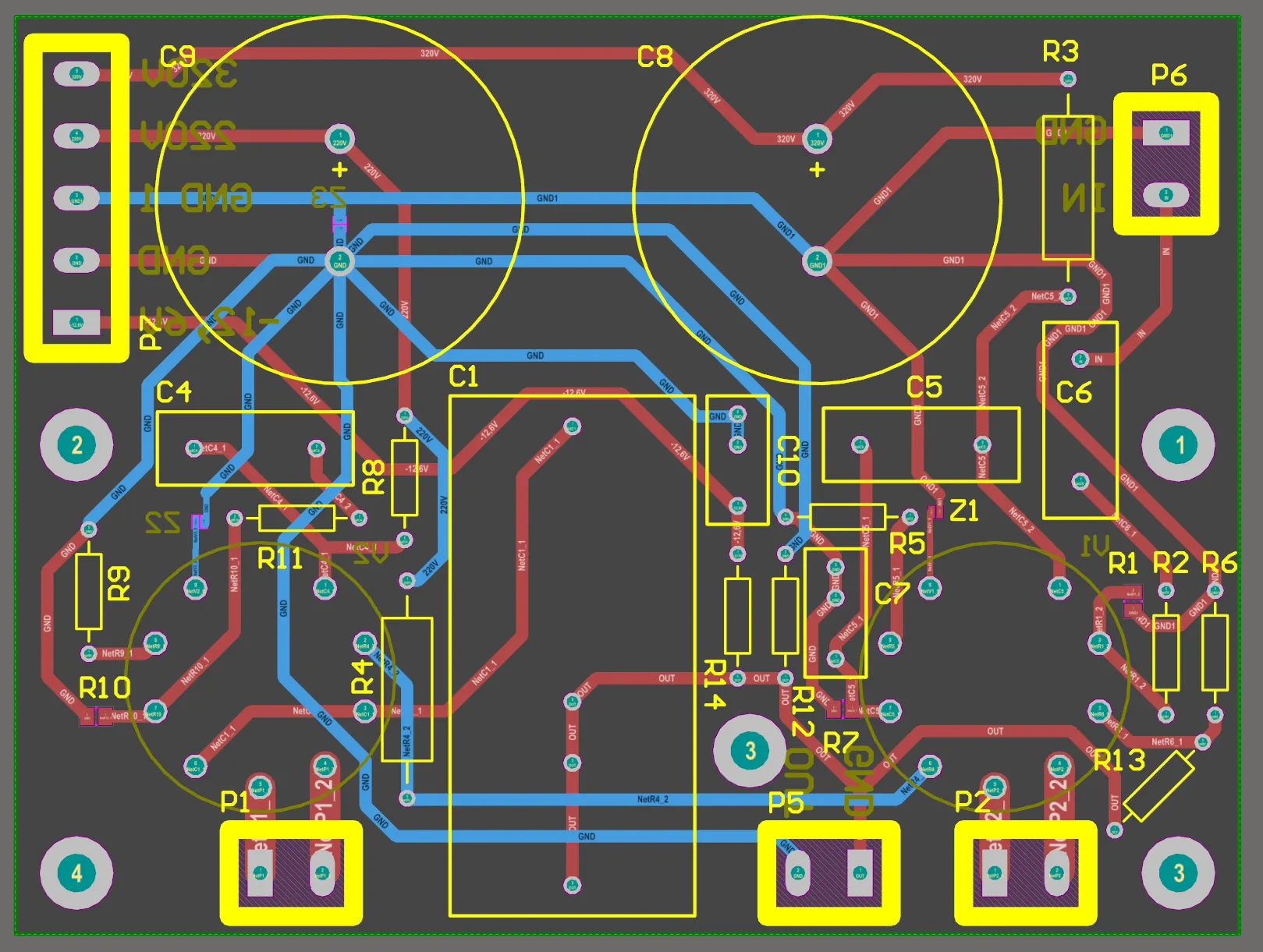
Grounding Fundamentals and Its Critical Role in Electrical and Electronic Systems

Understanding Ground in Electronic Circuits: Digital Ground vs. Analog Ground

Should You Use Solid or Hatched Copper Pour on PCBs?
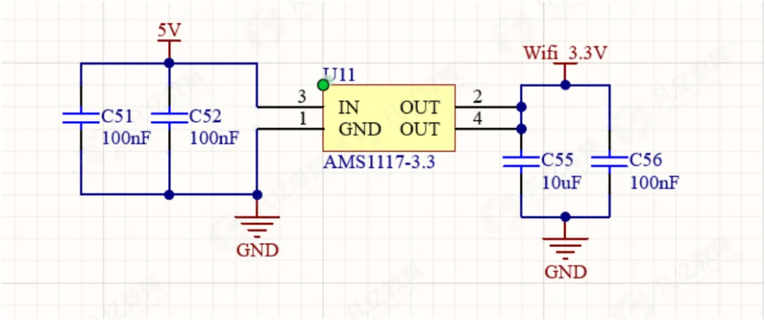
PCB Design Essentials for LDO Power Supplies
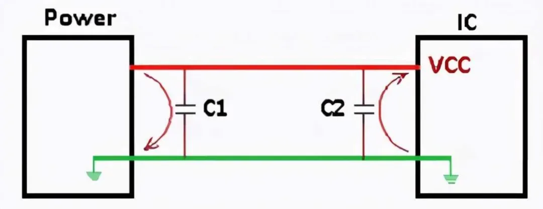
Why Two Capacitors? The Engineering Roles of 0.1 μF and 0.01 μF on the Power Rail

Why Do Eye Diagrams Collapse Even When High-Speed Interface Traces Are Length-Matched?
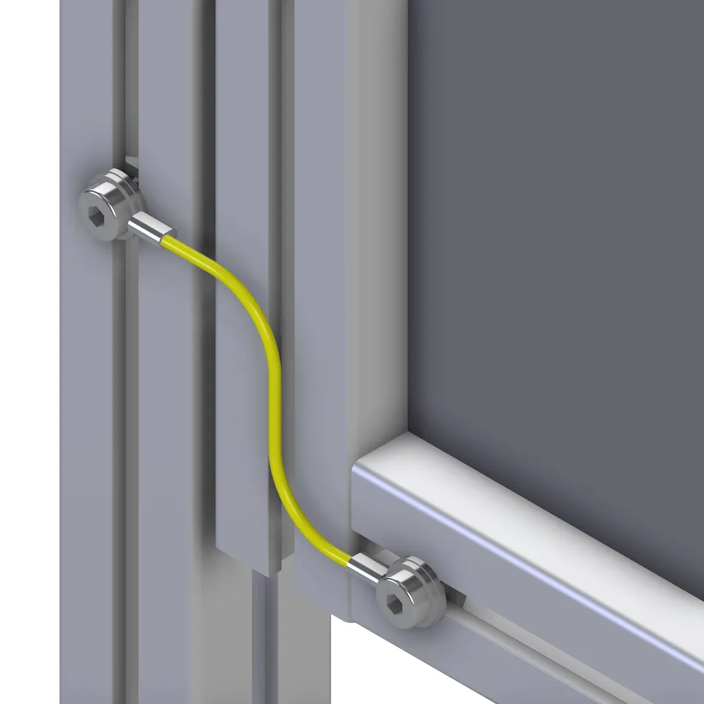
ESD Isolated Conductors: Definition and Measurement for SMT Engineers
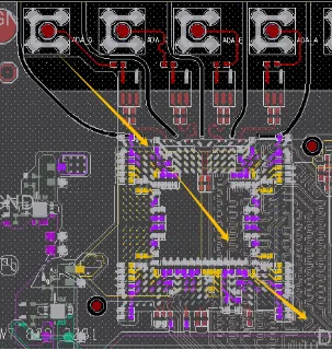
Mixed-Signal PCB Layout and Routing Design

When Is It Worth Keeping a Power Plane on a Four-Layer PCB?
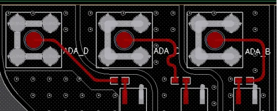
Mitigating Interference in Mixed-Signal PCB Design
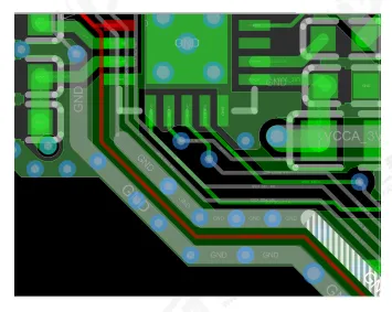
PCB Design Guidelines for Audio Interface Circuits
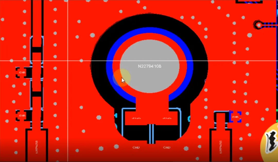
Why Designers Often Tie PCB Ground to Chassis Ground with a Parallel Resistor and Capacitor
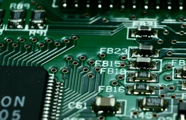
Maintaining PCB Signal Integrity in Harsh Environments: Challenges and Practical Guidelines
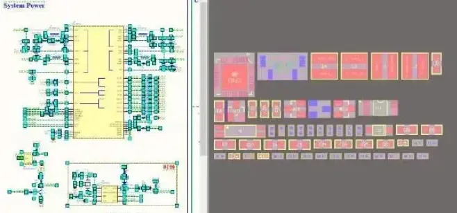
Boost PCB Design Efficiency with Interactive Cross-Probing and Modular Placement

Adding Via Stitching in KiCad with the kicad-action-scripts Plugin
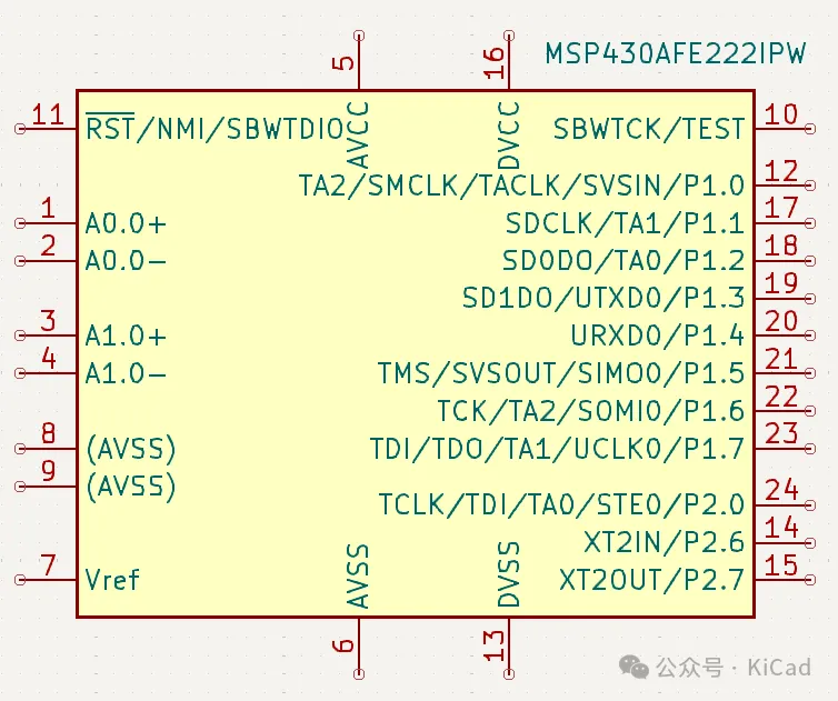
Using Alternate Pins in KiCad
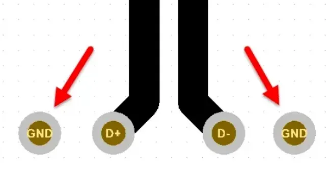
USB Interface PCB Design Guide: From Type-C to High-Speed Routing
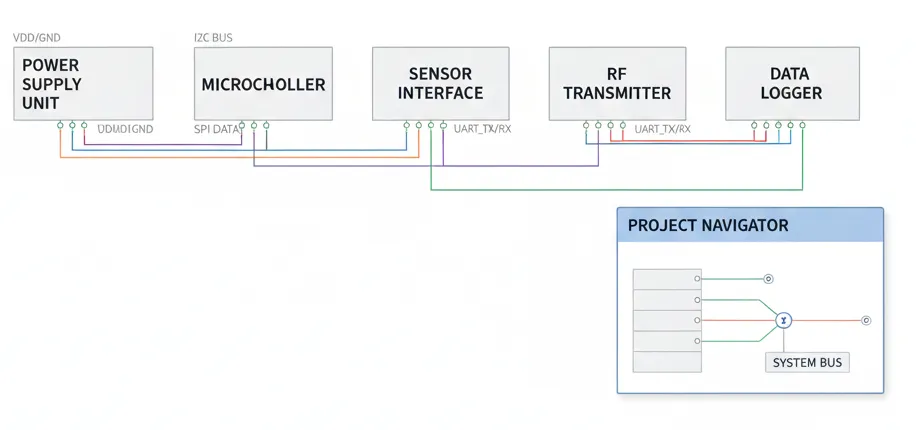
KiCad Finally Supports Flat (Tiled) Schematic Structure!