This article summarizes practical, field-proven guidelines for laying out and routing mixed-signal PCBs. The core objective is to minimize coupling between analog and digital domains, control return paths, and preserve both signal integrity and power integrity across the board.
Design Guidelines for Mixed-Signal Boards
-
When a design includes both analog and digital circuits, prioritize the layout and routing of the analog sections. Optimize placement, routing, and grounding to minimize interference to sensitive analog nodes and to reduce susceptibility to digital noise.
-
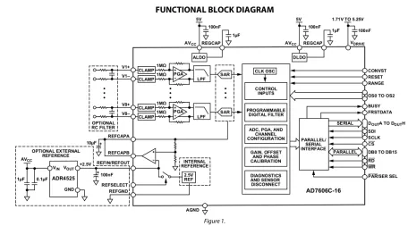
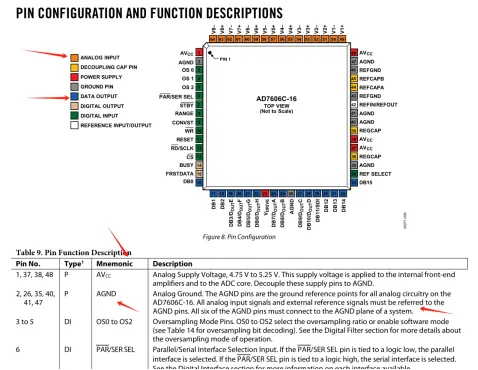
Before placement, analyze and partition the digital and analog circuits. Place digital devices and analog devices in distinct functional regions. Whether to split analog ground (AGND) and digital ground (DGND) should follow the relevant device datasheet and the schematic. Many modern ADC reference designs use a unified digital ground, but the PCB layout should still enforce functional partitioning to reduce interference. In mixed-signal sections using ADC or DAC devices, the split line often aligns with the device’s pinout; consult the datasheet and classify signals accordingly.
-
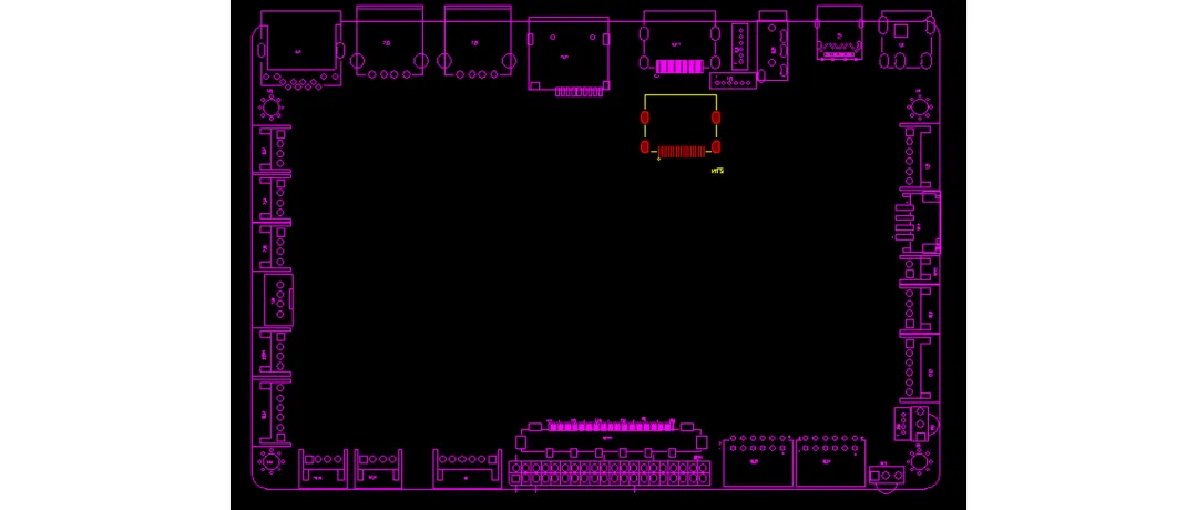
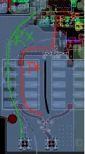
Analog devices are often placed near the board edge to align with analog interface connectors. If the customer has not specified the analog connector locations, keep analog interfaces away from power connectors and digital interfaces (for example, UART, Ethernet, HDMI). Separate analog receive and transmit connectors from each other.
-
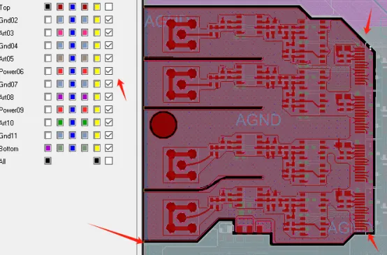
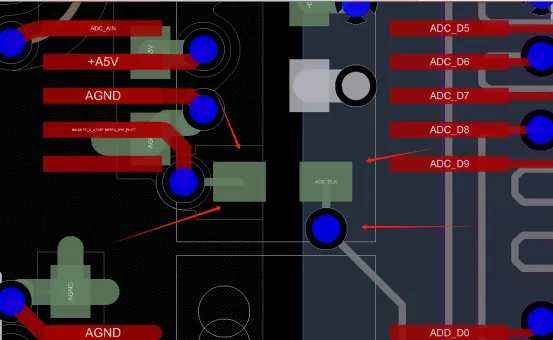
If the schematic separates AGND and DGND, maintain that separation on all layers for both signal and power routing. Avoid crossing a ground split with any signal or power trace. Power rails should also avoid crossing splits; if a power must cross, use a ferrite bead or a Pi filter to connect across the boundary. Keep the split gap at least 20 mil.
-
If isolation is implemented only by adding ferrite beads in the power rails, the power return path can become long. Add a second ferrite bead bridging AGND and DGND near the analog power bead to provide a controlled return path for the analog and digital power currents.
-
When a single signal must cross a split, you can add a ferrite bead or a 0 Ω jumper in series to control the crossing. For multiple signals crossing, concentrate the digital lines and provide a single controlled bridging point.
-
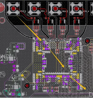
Plan placement according to signal flow. Arrange small analog signals first (typically low-level inputs from interfaces), then large analog signals (after amplification or at the ADC), and finally digital signals (FPGA/DSP/CPU). This supports short, clean paths and simplifies return control.
-
Place the A/D converter straddling the analog and digital partitions. Typically, tie AGND and DGND together at the ADC per the datasheet guidance to control return currents at the conversion boundary.
-
Common analog devices and signals include RGB video signals; IF inputs via BNC or SMA connectors; audio and microphone circuits; op-amps, comparators, and filters; infrared and thermal sensors, Bluetooth-related sensors; crystals; RF antennas and RF switches. Treat these as analog or RF-critical circuits and separate them from noisy digital sections.
-
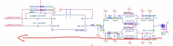
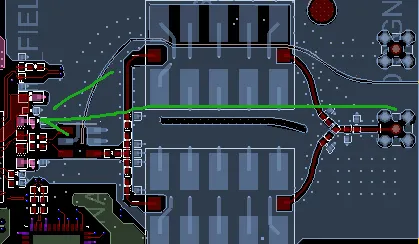
Follow the schematic functional order during placement and routing. For analog device power pins, place both bulk and high-frequency decoupling capacitors. Prefer routing the power through the capacitors before reaching the device pins. Use at least 20 mil width for analog power traces. For fine-pitch pins, match the escape trace width to the pin width until reaching the decoupling capacitor or via.
-
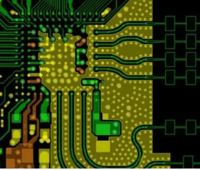
Where space permits, guard sensitive analog traces with grounded shielding (guard traces or ground pour). Add stitching vias along the guard at intervals not less than 200 mil to maintain a low-impedance connection to the reference plane.
-
Avoid vias in analog signal paths where possible; use trace widths above 10 mil. For 50 ohm analog lines, ensure a continuous reference plane (interlayer referencing) and avoid stubs. Route through protection components (for example, ESD devices) before exiting to connectors or long runs.
-
Keep switching power regulators, clock circuits, and high-power components away from analog circuits and sensitive analog traces.
-
For baluns (balanced-to-unbalanced converters), control the input and output impedance per design. Follow the schematic for the ground configuration on both sides of the balun; in most cases, there is no ground split at the balun.
-
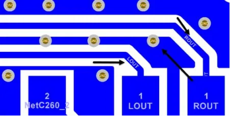
For RGB signals, increase the line width to more than 10 mil and provide ground shielding. When these signals must cross a split, adding ferrite beads is generally recommended. For BNC/SMA signal pins, clear copper on all layers beneath the pins, with a clearance at least 20 mil from the pad. Route audio left/right channels with 10 mil/10 mil width/spacing; apply the same to MIC+ and MIC?.
-
Op-amps, comparators, and filters typically do not require controlled impedance. Use 10 mil trace widths and adopt a straight, linear "I-shaped" flow in overall placement and routing to maintain clarity and minimize coupling.
-
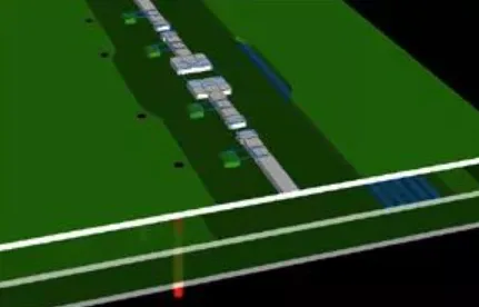
For IF signals, use interlayer referencing to achieve 50 ohm impedance while keeping traces as wide as possible to reduce attenuation. Under antennas, remove copper (copper keepout) and open the solder mask as required; maintain a clearance region preferably greater than 5 mm.
-
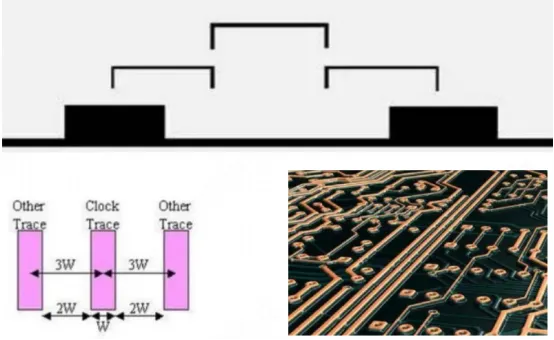
Separate digital receive and transmit routing. Avoid placing Rx and Tx on the same layer when possible. If they must be on the same layer, maintain the 3W rule (spacing at least three times the trace width) between Tx–Tx and Rx–Rx pairs, and the 5W rule between Rx and Tx lines to reduce crosstalk.