Signal integrity on printed circuit boards has become a central design concern as products grow smaller while performance requirements continue to rise. The convergence of IoT and AI accelerates this trend: package sizes shrink, functional density and switching speeds increase, and susceptibility to electromagnetic interference grows. Even in severe environmental conditions—temperature extremes, humidity, vibration, and strong electromagnetic fields—robust signal integrity can be achieved through disciplined engineering practice. This article summarizes practical methods that have proven effective in demanding applications.
1. Material Selection Is Foundational
Signal integrity starts with the materials you choose—both for components and the PCB substrate. Low-loss laminates reduce dielectric loss and help preserve edge rates and amplitude at high frequency. Materials with lower dielectric constant (Dk) and low loss tangent (Df) minimize dispersion and attenuation, improving high-speed channel performance and reducing susceptibility to interference.
Environmental resilience is equally important. In humid or condensing environments, some substrates absorb moisture, which raises effective Dk and Df, increases loss, and can shift controlled impedance outside tolerance. Moisture uptake also increases leakage and can precipitate conductive anodic filament (CAF) risk over time. Selecting substrates with low moisture absorption, stable Dk and Df over temperature, and appropriate glass transition temperature (Tg) and coefficient of thermal expansion (CTE) can significantly improve reliability. Advanced polymer systems with low dissipation factor (for example, loss tangent as low as 0.001 at 10 GHz) are gaining adoption in high-frequency designs. While these materials command a premium, they often pay for themselves in mission-critical or harsh-environment applications where signal margin and long-term stability are essential.
Beyond the laminate, consider conductor surface roughness and copper foil type, as roughness contributes to additional high-frequency loss. Solder mask and conformal coatings also affect impedance and loss at microwave frequencies. In severe environments, coatings are often used for environmental protection; choose formulations compatible with the SI needs of your design and verify their effect with test coupons or controlled prototypes.
2. Optimize Trace Geometry and Length
Routing discipline is a primary lever for reducing loss and crosstalk. Excessively long or unnecessarily wide traces increase capacitive loading, radiation, and coupling. Keep signal paths as short as practical, maintain consistent reference planes, and design compact return loops to minimize loop inductance. Controlled-impedance routing with appropriate stackup ensures predictable characteristic impedance for single-ended and differential interconnects.
Key layout practices include:
- Maintain adequate spacing to reduce capacitive and inductive crosstalk, especially for long parallel runs.
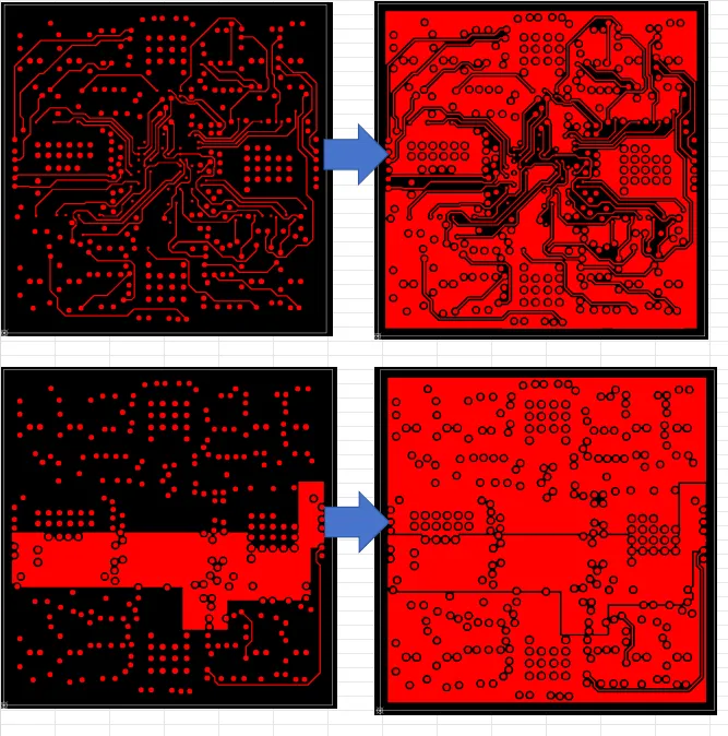
- Avoid routing high-speed lines over plane splits or gaps; preserve a continuous return path and provide stitching vias when layer transitions are unavoidable.
- Manage vias thoughtfully. Shorten via stubs and, for critical high-speed nets, consider backdrilling or blind/buried vias to reduce reflections and resonances.
- For differential pairs, control trace width, spacing, and symmetry; minimize skew by careful length matching and consistent layer transitions.
Additive manufacturing and other advanced fabrication techniques can enable microfine features and new routing topologies. With 3D printing of conductive traces, designers can realize compact, direct paths that circumvent mechanical constraints of traditional machining or slotting. If pursuing such approaches, validate achievable feature sizes, conductivity, thermal stability, and variation across environmental extremes before committing to production.
3. Grounding and Decoupling Strategy
Grounding practices are pivotal in high-frequency circuits. Solid ground planes provide a low-impedance return path and reduce common-impedance coupling. Multi-point grounding across the board, with low-inductance stitching vias near layer transitions and across discontinuities, helps contain return currents and suppress EMI. Where mixed-signal isolation is required, separate regions for analog and digital domains can be effective; however, over-aggressive ground splits can create return-path discontinuities that degrade signal integrity. If grounds are partitioned, provide controlled, low-impedance connections at appropriate locations to guide return currents.
Power-distribution decoupling must be designed as a network rather than as discrete, isolated capacitors. Place decoupling capacitors as close as physically possible to the device power pins, minimize via inductance, and distribute values to cover the intended frequency band of PDN noise. The capacitor selection should consider effective series resistance (ESR) and effective series inductance (ESL), as these determine impedance minima and anti-resonance peaks. Use multiple mounting vias for critical capacitors and ensure tight loop area. In some high-frequency contexts, RC snubbers or damping resistors are introduced at specific sources or loads to tame resonances; this is highly application-specific and should be guided by measurement or simulation.
4. Thermal Management Matters
Thermal control is an integral part of signal integrity because temperature changes both dielectric and conductor properties. As temperature rises, conductor resistivity increases and losses grow; dielectric constants and loss tangents drift; timing can shift; and jitter can worsen. In dense, power-intensive boards, combine heat sinks and heat spreaders with thermal vias and thermal pads to pull heat away from sensitive circuits. Allocate placement to distribute hot components, align with airflow, and avoid trapping heat in enclosures.
Mechanically, repeated thermal cycling stresses solder joints and vias due to CTE mismatch; microcracks or intermittent contact can introduce intermittent SI problems that are difficult to diagnose. Use appropriate land patterns, consider underfill or mechanical support for large packages, and avoid routing critical nets through areas subject to thermal gradients or flexure.
5. EMI Shielding and Filtering
Shielding and filtering form the outer defense against interference in high-frequency PCBs. Board-level shielding cans, high-conductivity meshes, and elastomeric gaskets can attenuate radiated emissions and improve immunity, particularly around RF circuits and sensitive analog front-ends. When implementing shields, ensure robust ground contact around the shield perimeter, minimize slotting, and account for venting or apertures, which can become leakage points or resonant structures.
Complement shielding with appropriate filtering. For signal lines, common-mode chokes and well-placed RC/LC filters reduce conducted interference while preserving required bandwidth. For high-power equipment, three-phase input filters provide comprehensive conducted-noise suppression across phases and to ground. Keep filter leads and connections short, place them close to connectors, and observe proper line-to-line and line-to-ground component orientation to avoid introducing new coupling paths. Careful partitioning of dirty (noisy) and clean (quiet) zones on the PCB reduces re-injection of filtered noise into sensitive circuits.
6. Comprehensive Design Verification and Test
Simulation and measurement must go hand in hand to qualify designs for severe environments. Electromagnetic and circuit co-simulation during design can predict impedance profiles, resonances, and coupling; thermal simulations can identify hotspots and guide heat-spreading strategies. Still, bench validation is essential to capture real-material behavior, manufacturing variation, and environmental effects.
Representative verification steps include:
- Impedance control verification using time-domain reflectometry (TDR) on coupons and critical interconnects.
- S-parameter measurement for high-speed channels to validate loss, return loss, and crosstalk against budgets.
- Pre-compliance EMI scans to identify dominant emission lines and coupling mechanisms before final certification.
- Environmental testing aligned with application requirements. For example, MIL-STD-810 requires validation under temperature extremes, thermal cycling, vibration, mechanical shock, humidity, and other stressors to ensure performance aligns with expectations in field conditions.
- On-bench stress testing of PDN impedance and transient response, including load steps at temperature extremes.
Plan measurement points and diagnostic hooks into the design—test pads, optional components for damping or filtering, removable shields—to accelerate troubleshooting and allow rapid iteration if issues arise.
7. Leveraging AI in the Design Flow
AI-assisted tools are increasingly capable of accelerating PCB design. They can identify layout bottlenecks, propose routing and placement alternatives, and optimize PDN networks under complex constraints. In some reported cases, teams have used AI to significantly improve chip or board-level performance within compressed timelines while reducing power consumption.
However, AI-generated solutions must be treated with the same rigor as any design. Train and validate models against relevant datasets, enforce electrical and mechanical constraints explicitly, and corroborate AI recommendations with simulation and lab measurements. Use AI as a design-space exploration assistant, not a substitute for engineering judgment; final sign-off should rest on verified signal-integrity, power-integrity, thermal, and EMI performance evidence.
Continuous Improvement
As device functionality and environmental demands intensify, maintaining signal integrity on PCBs will remain challenging. The practices outlined above—careful materials selection, disciplined routing, robust grounding and decoupling, effective thermal design, prudent shielding and filtering, and thorough verification—provide a repeatable framework for building reliable systems. Staying current with advances in materials, fabrication, and design automation tools can unlock additional margin and resilience in the next generation of harsh-environment electronics.
Practical Checklist for Harsh-Environment Signal Integrity
- Substrate: Choose low-Df, low-moisture-absorption laminates with stable Dk/Df across temperature; validate copper roughness and coating effects.
- Stackup: Define controlled-impedance geometry; ensure continuous reference planes; plan return paths and stitching vias.
- Routing: Shorten critical nets; minimize parallelism; control differential parameters; manage via stubs and transitions.
- Grounding: Use solid planes and local stitching; avoid problematic splits; provide controlled analog/digital isolation when required.
- PDN: Place decoupling caps at power pins; minimize loop inductance; distribute capacitor values to cover target frequency bands; damp anti-resonances as needed.
- Thermal: Use heat spreaders, thermal vias, and airflow management; avoid thermal stress on critical nets and interconnects.
- EMI: Implement shields with reliable ground contact; place filters at interfaces; partition noisy and quiet zones.
- Validation: Combine EM/SI/PI/thermal simulations with lab measurements; include environmental testing to relevant profiles and margins.
- Tooling: Employ AI/automation for exploration and optimization; verify outputs through established engineering workflows.
By integrating these practices early and continuously refining them through test feedback, teams can achieve robust signal integrity even when the environment is anything but benign.