










Ground is a foundational concept in electronics. In every practical circuit, measurements, analysis, and functional behavior are all referenced to some common point. Knowing what "ground" actually means in a circuit, why multiple grounds may exist, and how to handle digital and analog grounds on a PCB is essential for reliable design.
What Does "Ground" Mean in an Electronic Circuit?
In an electronic circuit, ground is a designated common reference node used to define voltage at every other point. All node voltages in a circuit are expressed relative to this reference. By convention, this reference is set to 0 V. This does not imply that the ground node is physically connected to the earth or that it is the lowest potential in an absolute sense—it is simply the chosen reference for measurement and operation.
When you assign a ground node in a circuit, you can immediately determine the voltages at other nodes with respect to this reference. This is what allows us to say a node is "5 V" or "-12 V": those values are relative to the declared ground reference.
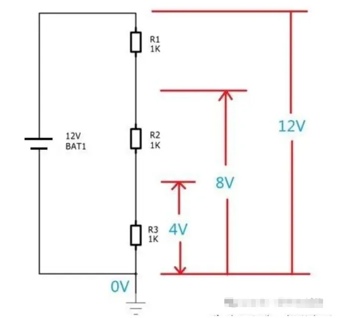
Figure | Ground as the common reference and example node voltages
Ground set to 0 V does not necessarily mean it is the lowest potential in the system. Consider a dual-supply circuit that provides +12 V and -12 V relative to ground. Here, ground is still 0 V by definition, but -12 V is a lower potential than ground. Current directions are typically denoted relative to the ground reference, and each supply returns its current to its source through its own loop.
A single system can be partitioned into many functional subcircuits, and each subcircuit can be analyzed using its own local reference. In other words, a complex design can have multiple "grounds" when viewed as separate functional blocks. This is often done to make analysis and measurement convenient, and later those local references are tied together at specific points for proper operation.
For example, several subcircuits may share a component such as a current-sense resistor. You might define one local ground (Reference Ground 2) for those subcircuits to make the loop analysis straightforward, while a separate reference (Reference Ground 1) is used for the current measurement circuitry if the input signal to that block is defined relative to Reference Ground 1. The key is that the choice of reference serves clarity and correct operation; later, the layout and grounding strategy ensure safe and controlled connections between these references.
What Are Digital Ground and Analog Ground?
Digital ground (DGND) is the reference node for digital circuitry, and analog ground (AGND) is the reference node for analog circuitry. The reason designers distinguish them is to control how noise and return currents flow, thereby reducing cross-domain interference. Digital inputs can be high impedance and sensitive at certain nodes, and analog circuits are often sensitive to high-frequency switching noise from digital domains. Separating references and controlling where and how they connect helps maintain signal integrity and stable operation.
When there is no electrical connection between two ground references, the related signal paths are also galvanically isolated. Signals cannot be directly transferred across the isolation boundary because they do not share a reference. In these cases, transformers or optocouplers are used to pass information across the boundary while maintaining isolation.
How Is "Ground Isolation" Implemented When Grounds Are Connected?
Ground "isolation" in many mixed-signal designs does not necessarily mean a complete galvanic break. Instead, it means separating current return paths so that digital and analog return currents do not share the same impedance in ways that inject noise into sensitive circuitry. In other words, what we isolate is the return current loops of different domains, even when their grounds are ultimately connected at a defined point.
This is primarily a PCB layout task. A common approach is to partition the ground plane and control how return currents from the digital and analog sections flow back to the primary input filter and bulk capacitor. Each domain's return current is guided along its own path to a carefully chosen common point, rather than allowing high-frequency return currents to spread across sensitive areas.
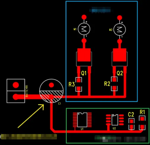
Figure | Ground isolation by guiding digital and analog returns to the input filter/bulk capacitor along separate paths
In the example above, the digital and analog sections return to the input filter/bulk capacitor through different routes. This achieves two objectives: it keeps noisy digital return currents from flowing under sensitive analog circuitry, and it gives analog signals a quiet, low-impedance return path. This is often called single-point or star grounding for mixed-signal systems when done at a defined node.
For tighter control, designers often bridge the ground partitions at a single location using either a 0 Ω resistor or a ferrite bead, and then route the combined return to the common point. These components let you control where the return currents converge and at what frequencies they can cross between domains.
Bridging Grounds with a 0 Ω Resistor
A 0 Ω resistor provides a deliberate, narrow current path between ground regions. Compared with a wide copper link, a 0 Ω resistor constrains the width of the current path, which helps limit loop area and reduces the chance of sudden loop-current spikes coupling into nearby circuitry. It also gives flexibility during bring-up: if measurements suggest the bridge location should change, a 0 Ω link can be easily moved or depopulated to test alternative configurations.
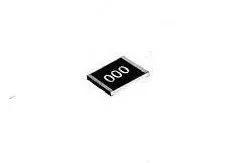
Figure | Example 0 Ω resistor component
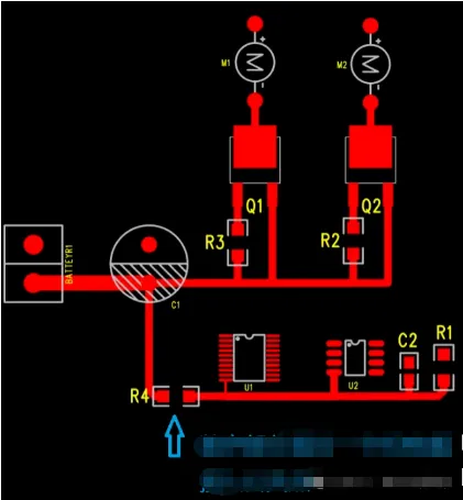
Figure | Using a 0 Ω resistor as a controlled bridge between ground regions
When using a 0 Ω bridge, it should be placed at the intended single-point connection, typically near the input filter/bulk capacitor or at another well-chosen common node. Avoid placing this bridge where high-speed signal traces would have to cross a ground split, as that would force their return currents to detour, increasing loop area and radiated/conducted noise. The goal is a short, direct return path for high-frequency currents.
Bridging Grounds with a Ferrite Bead
A ferrite bead behaves like a small inductor with frequency-dependent impedance. It provides very low DC resistance so the DC ground reference is shared, but it presents higher impedance to high-frequency noise, attenuating unwanted coupling between domains. In effect, a bead helps "pass DC, block AC."
Used as a bridge between AGND and DGND, a bead can reduce the flow of high-frequency digital noise into the analog ground region. However, because its impedance is frequency-dependent, it should be selected with the expected noise spectrum in mind. Place the bead at the designated single-point connection and keep the path to the common return node as short and direct as possible.
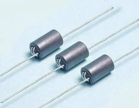
Figure | Example ferrite bead component
When Grounds Are Not Electrically Connected
In some designs, complete galvanic isolation between ground domains is required—for example, to meet safety requirements or to break ground loops between equipment. In these cases, there is no direct electrical connection between the grounds, and signals cannot be referenced across the boundary. Information transfer is achieved using isolation components such as transformers or optocouplers. The isolation barrier ensures that return currents in one domain cannot flow in the other, while still allowing data or control to pass across.
Practical Takeaways for Mixed-Signal PCB Design
- Ground is a reference node defined as 0 V for the purpose of measurement and operation; it is not necessarily the lowest absolute potential.
- Complex systems often benefit from separate local references (e.g., AGND and DGND) to manage return paths and minimize cross-domain coupling.
- When AGND and DGND must connect, use a well-defined single-point connection and guide returns to the input filter/bulk capacitor by separate paths.
- Use a 0 Ω resistor or a ferrite bead at the bridge to control where and at what frequencies the domains interact. Place the bridge to avoid forcing high-speed traces to cross a split.
- For complete isolation, use galvanic isolation (transformers, optocouplers) and maintain separate ground references with no direct electrical connection.
By defining the reference node clearly, controlling return paths on the PCB, and choosing appropriate bridging or isolation techniques, you can significantly improve signal integrity in mixed-signal systems and reduce the risk of noise coupling that degrades performance.






