Introduction
Power supply PCB trace routing demands careful consideration to ensure reliable performance under high electrical loads and varying operating conditions. Engineers must balance power delivery efficiency with signal integrity, particularly in designs involving converters, regulators, and distribution networks. Key aspects include determining the appropriate power supply PCB trace width for current handling, managing power supply PCB trace impedance for control signals, optimizing power supply PCB high current traces to minimize losses, and isolating power supply PCB signal traces from noise sources. Poor routing can lead to overheating, voltage drops, electromagnetic interference, and premature failure. This article outlines structured best practices grounded in engineering principles to guide electric engineers in creating robust power supply layouts. By following these guidelines, designs achieve compliance with industry standards and enhanced longevity.
Why Proper Trace Routing Matters in Power Supply PCBs
In power supply circuits, traces carry substantial DC currents alongside sensitive feedback and switching signals, making routing a pivotal factor in overall system reliability. Inadequate power supply PCB trace width results in excessive resistance and heat generation, potentially degrading components or violating thermal limits. Similarly, uncontrolled power supply PCB trace impedance can distort high-frequency signals, leading to instability in switching regulators. Power supply PCB high current traces, if not properly sized, amplify risks of electromigration and board-level failures over time. Signal traces in proximity to power paths suffer crosstalk and ground bounce, compromising control loop performance. Adhering to established design principles prevents these issues, ensuring the power distribution network supports peak loads without compromise.
Effective routing also supports electromagnetic compatibility by reducing loop areas and radiated emissions. Compliance with standards like IPC-2221 for general PCB design reinforces these practices across manufacturing variations. Ultimately, thoughtful trace strategies extend product lifespan and reduce field returns in demanding applications such as industrial power systems and telecommunications equipment.
Fundamental Principles of Trace Width and Current Capacity
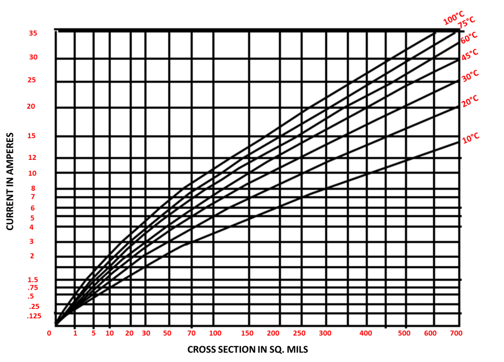
Power supply PCB trace width directly influences the current-carrying capacity, governed by factors like copper thickness, ambient temperature, and allowable temperature rise. Wider traces reduce resistance per unit length, calculated as R = ρ * L / (W * T), where ρ is copper resistivity, L length, W width, and T thickness. However, excessive width consumes board space and increases capacitive coupling risks. Engineers reference IPC-2152 to determine widths that limit temperature rise to safe levels, typically 10 to 20 degrees Celsius above ambient for external traces. Internal traces demand wider dimensions due to poorer heat dissipation through surrounding dielectrics. This principle ensures power supply PCB high current traces handle peak currents without hotspots.
Thermal management extends to via usage and plane integration, as traces alone may insufficiently conduct heat in multilayer boards. Voltage drop across traces, ΔV = I * R, must stay below 5% of supply voltage to maintain regulation accuracy. Simulations validate these calculations, accounting for dynamic loads in power supplies.
Managing Trace Impedance in Power Supply Designs
Power supply PCB trace impedance control is essential for high-speed signal traces involved in pulse-width modulation, current sensing, and communication interfaces. Characteristic impedance Z0 depends on trace geometry, dielectric constant, and stackup configuration, following transmission line theory. Microstrip traces on outer layers exhibit higher impedance than striplines due to air-dielectric interfaces. IPC-2141 provides guidelines for calculating and tolerating impedance variations within 10% for most applications. In power supplies, mismatched impedance causes reflections, ringing, and overshoot on gate drive signals. Maintaining consistent width, spacing, and reference plane proximity achieves target values like 50 or 100 ohms.
Reference planes, typically ground or power pours, form controlled return paths, minimizing inductance. For differential signal traces, symmetric routing preserves balance and common-mode rejection. Fabricators adjust etch tolerances and material properties to meet specs, underscoring the need for precise design files.
Strategies for High Current Traces in Power Supplies
Power supply PCB high current traces require prioritization of low resistance paths from input capacitors to loads, often using 2 oz or thicker copper. Multiple parallel traces or fused configurations distribute current evenly, reducing individual stress. Shortening trace lengths minimizes I2R losses, especially in high-power density designs. Vias in arrays provide interlayer transitions, sized to match trace ampacity with plating thickness considered. Pouring copper planes for primary rails offers superior performance over discrete traces, with stitching vias for current sharing. These approaches align with IPC-2221 recommendations for conductor sizing in multilayer boards.
Heat dissipation demands airflow paths and thermal reliefs at pads to prevent solder joint failures. In dense layouts, interleaving power and ground planes reduces inductance. Monitoring tools during layout verify compliance before fabrication.
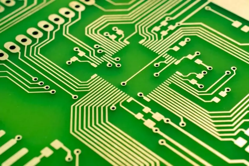
Best Practices for Signal Trace Routing Near Power Paths
Power supply PCB signal traces must avoid parallel runs with high current paths to suppress inductive and capacitive coupling. Orthogonal routing or dedicated signal layers isolate them effectively. Ground planes shield sensitive traces, providing low-impedance returns. Length matching for clock and data lines prevents skew in digital controls. Avoiding right-angle bends reduces reflections, favoring 45-degree mitered corners. Reference plane splits demand stitching capacitors nearby to maintain continuity.
Guard traces or moats further enhance isolation in mixed-signal power supplies. Differential pairs benefit from tight coupling and impedance matching. These practices ensure clean signal waveforms amid noisy power environments.
Integrating Planes and Vias for Optimal Performance
Power planes supplant traces for main power distribution, offering uniform low resistance and inherent decoupling. Partial pours suffice for secondary rails, connected via arrays of vias. Via current capacity follows similar rules as traces, scaled by barrel dimensions. Decoupling capacitors bridge plane splits, injecting high-frequency currents locally. Layer sequencing alternates power, ground, and signal for balanced fields. This stackup strategy minimizes crosstalk and supports impedance targets.
Thermal vias under hot components wick heat to inner planes. Design reviews confirm via densities prevent bottlenecks.
Common Challenges and Troubleshooting Tips
Overheating in power supply PCB high current traces often stems from underestimated peak currents or external trace heating. Thermal imaging post-prototype identifies hotspots for redesign. Voltage droop signals insufficient power supply PCB trace width, prompting recalculations per IPC-2152. Signal distortion traces to impedance discontinuities, resolved by consistent geometries. EMI failures indicate poor return path integrity, fixed with enhanced stitching. Iterative simulations and test boards refine layouts.
Fabrication variances like etch shrinkage affect impedance, necessitating test coupons. Documentation of assumptions aids future iterations.
Conclusion
Mastering power supply PCB trace routing hinges on systematic application of width sizing, impedance control, and isolation techniques. Power supply PCB high current traces demand robust dimensions and plane support, while power supply PCB signal traces require shielding and matching. Integrating standards like IPC-2152 and IPC-2141 ensures designs withstand real-world stresses. Electric engineers benefit from layered planning, from stackup to verification. These best practices yield efficient, reliable power supplies with minimal rework. Prioritizing these elements elevates design quality across projects.
FAQs
Q1: How do I calculate power supply PCB trace width for high currents?
A1: Determine required power supply PCB trace width using current, copper weight, and temperature rise limits from IPC-2152 charts or equations. Account for external versus internal layers, as internal traces need wider dimensions for equivalent capacity. Verify with simulations incorporating board thickness and airflow. This prevents overheating and voltage drops in power distribution networks.
Q2: Why is power supply PCB trace impedance critical for signal integrity?
A2: Power supply PCB trace impedance affects signal propagation speed and reflection in control and feedback paths. Maintain consistent Z0 through uniform width, spacing, and reference planes per IPC-2141 guidelines. Mismatches cause ringing on switching signals, degrading efficiency. Test coupons confirm fab tolerance during production.
Q3: What are key tips for routing power supply PCB high current traces?
A3: Use wide power supply PCB high current traces, short paths, and multiple vias to minimize resistance and inductance. Prefer planes for primary rails with stitching for returns. Parallel traces distribute load evenly. Thermal reliefs and airflow paths manage heat effectively.
Q4: How to separate power supply PCB signal traces from high current paths?
A4: Route power supply PCB signal traces orthogonally or on isolated layers with ground shielding. Employ guard traces and avoid splits without capacitors. Maintain differential balance for pairs. This reduces crosstalk and preserves waveform fidelity in noisy environments.
References
IPC-2152 — Standard for Determining Current Carrying Capacity in Printed Board Traces. IPC
IPC-2221 — Generic Standard on Printed Board Design. IPC
IPC-2141 — Controlled Impedance Design Guide for High Speed Digital Signals. IPC
IPC-6012E — Qualification and Performance Specification for Rigid Printed Boards. IPC, 2017


