










Universal Serial Bus (USB) has evolved from USB 1.0 low-speed links to the 10 Gbps era of USB 3.1 while adding power delivery capability up to 100 W. The Type-C connector, with reversible insertion and broad compatibility, has become the mainstream choice for mobile devices and laptops. As data rates increase, PCB design must satisfy tighter signal integrity (SI) and electromagnetic interference (EMI) constraints. This guide consolidates practical design techniques for USB interfaces, from placement and protection to high-speed differential routing and Type-C specifics.
Layout Fundamentals: Get the Basics Right
Connector Placement and ESD Protection
-
Near the board edge: Place the USB receptacle near the PCB edge, typically extending 3–5 mm beyond the board outline to ensure reliable insertion and removal.
-
ESD and common-mode choke placement: Place the ESD protection device as close to the connector pins as possible (≤ 1.5 mm). Follow it with a common-mode choke and any RC filtering. Keeping the protection and choke close to the connector minimizes stub lengths and reduces the energy reaching downstream circuitry, improving both SI and EMI performance.
Note: Maintain a safe clearance between the ESD device and the connector shield to avoid heat damage during shell soldering and to ensure robust mechanical assembly.
Protective Ground Isolation
When the connector’s mechanical stakes or shield tabs tie to protective ground (PGND), maintain a 2 mm clearance from system ground (GND). Bridge PGND to GND using a ferrite bead to provide high impedance at high frequency while maintaining a DC return. This practice helps route ESD and surge currents directly to chassis/protective ground at the connector, reducing the noise injected into system GND.
Use abundant ground stitching vias in the protective ground region to lower return-path impedance and to confine ESD current loops locally. Dense via stitching also reduces ground bounce and suppresses radiated emissions from the shell connection area.
Differential Pair Routing: Impedance Control and EMI Suppression
Differential Impedance and Coplanar Grounding
Impedance requirements: Maintain 90 Ω differential impedance for USB 2.0 (±10%) and tightly control to 90 Ω for USB 3.0/3.1. Impedance control is achieved through the stackup, trace geometry, spacing, and reference plane configuration. Coordinate early with your PCB fabricator to define target dielectric thickness and copper weights to meet the impedance goals.
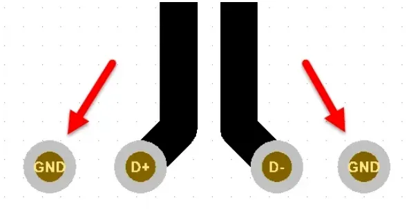
Coplanar ground guard: Use ground copper or ground traces flanking the differential pair on the same layer, with spacing ≤ 3× the trace width, to form a coplanar waveguide with ground. This structure helps contain fields, reduces coupling to adjacent structures, and mitigates radiated EMI. Note that adding side ground decreases differential impedance; compensate by adjusting trace width and spacing based on field-solver results.
Routing Layers and Reference Planes
-
Prefer inner-layer routing: Route high-speed differential pairs on inner layers over solid reference planes. Inner-layer routing reduces emissions by containing fields between the traces and the reference plane and provides a stable, continuous return path.
-
Avoid crossing plane splits: Do not route differential pairs across splits or cutouts in the reference plane. Crossing a split forces return currents to detour around the gap, causing impedance discontinuities, increased common-mode noise, and radiation.
Vias and Return Path Control
-
Minimize layer transitions: Each via introduces parasitic inductance and capacitance, which can degrade high-frequency performance. Limit differential pair layer transitions to no more than two where possible to reduce discontinuities and insertion loss.
-
Add return path vias: Place a pair of ground stitching vias adjacent to the differential signal vias at every layer transition. These stitching vias provide a short, low-impedance return path that confines current loops to a small area and reduces mode conversion and ringing.
These practices reduce differential-to-common-mode conversion, improve eye quality, and help the design pass EMI compliance without resorting to overly aggressive filtering that could impact signal integrity.
USB 3.1 High-Speed Design Techniques
Length Matching and Spacing
-
Intra-pair skew: Match the lengths within each differential pair tightly. Keep the length mismatch ≤ 5 mil; for USB 3.1, target ≤ 2 mil. Tight skew control minimizes phase mismatch and common-mode conversion, preserving the intended differential signaling and widening the eye opening.
-
Pair-to-pair spacing: Maintain spacing between pairs ≥ 4× the trace width to reduce crosstalk. Adequate separation limits near-end and far-end coupling, especially important when multiple high-speed interfaces coexist on the same board.
When length tuning is necessary, use short, broad meanders and avoid compact serpentine patterns with tight corners. Keep meanders on the same layer with a consistent reference plane and maintain coplanar ground to control impedance through the tuned sections.
Power and Signal Separation
-
Dedicated power region: Allocate a dedicated power area for VBUS (5 V/12 V/20 V) and avoid overlapping it with high-speed signal layers. Separating power distribution from sensitive routing helps minimize power-related noise coupling into the data paths.
-
Local decoupling: Place a 10 μF capacitor in parallel with a 0.1 μF capacitor close to the VBUS pin to filter a broad range of frequency content. The larger capacitor provides bulk energy storage, while the smaller capacitor addresses high-frequency transients.
Keep high-current paths short and wide, with clear returns to their source to avoid injecting magnetic flux into the high-speed regions. Where planes overlap or are stacked, ensure that the high-speed pairs always reference a continuous ground plane rather than a noisy power plane.
Type-C Interface: Design Considerations
CC Pins and Power Delivery (PD)
-
CC line routing: Route the CC pins as controlled-impedance lines and match their length with related signaling to ensure robust PD communication. Proper impedance control and clean reference reduce susceptibility to noise on the configuration channel.
-
VBUS path: For high-current delivery such as 20 V at 5 A, widen the copper to 80 mil or more and consider a mesh (grid) copper pattern to lower temperature rise while accommodating thermal reliefs during soldering. Apply multiple vias where VBUS transitions layers to distribute current and reduce localized heating.
Symmetrical Layout for Reversible Insertion
Type-C features 24 pins arranged to support reversible plug insertion. Use a symmetrical layout to minimize differences in signal path length and impedance between the two orientations. Symmetry helps equalize insertion loss, skew, and mode conversion regardless of cable orientation, simplifying compliance and improving interoperability.
Common Problems and Practical Fixes
Issue: Signal Ringing
-
Likely causes: Impedance discontinuities or incomplete return paths at layer transitions, connector breakouts, or areas where the reference plane is segmented.
-
Fixes: Add ground stitching vias near each differential via transition, verify the continuity of the underlying reference plane, and remove or reduce stubs by optimizing breakout geometry. Ensure that ESD and common-mode components do not introduce long stubs ahead of the high-speed channel.
Issue: EMI Test Failures
-
Likely causes: Routing high-speed pairs on outer layers without coplanar ground, inadequate ground containment, or long exposed sections near the connector.
-
Fixes: Route critical pairs on inner layers with solid ground reference, provide coplanar ground on both sides of the pair, and use shield cans near the connector when necessary. Improve ground stitching around the connector aperture and ensure the protective ground path for ESD currents is short and well-contained.
Conclusion
Reliable high-speed USB design hinges on disciplined layout and routing practices. Prioritize the fundamentals—connector placement, ESD proximity, and protective ground isolation—then enforce impedance control and field containment through inner-layer routing and coplanar ground. Pay meticulous attention to details like via transitions and return-path stitching, and maintain Type-C symmetry to support reversible operation. With these techniques, USB 3.1 and Type-C interfaces can achieve stable data transmission and high reliability while meeting stringent SI and EMI requirements.






