Have you ever lost time hunting for a component across dense schematic pages, or spent minutes scanning a crowded PCB to match a symbol to a footprint? When component counts rise and timeline pressure mounts, the ability to quickly correlate the schematic and PCB, and to organize placement by function, can make or break schedule and quality. This article presents two practical techniques that noticeably improve placement productivity and layout clarity: interactive cross-probing between the schematic and PCB, and modular placement using a defined area to rapidly arrange components.
The two methods complement each other. Cross-probing lets you locate and select the exact parts you intend to place as a group, while modular placement allows you to arrange those parts cleanly within a bounded region. Combined, they transform initial placement from a manual slog into a structured, repeatable workflow that keeps design intent visible throughout layout.
Interactive Placement: Schematic–PCB Cross-Probing
The essence of interactive placement is simple: see it, select it; select it, highlight it. When cross-probing (often called Cross Select Mode) is enabled in both the schematic and the PCB editor, selecting a component in one domain immediately highlights and selects the corresponding object in the other. This synchronous selection eliminates guesswork and navigation overhead.
In practice, this means you can identify a functional cluster on the schematic—say, a power regulation block, a sensor interface, or a memory subsystem—select that set of symbols, and instantly see the matching footprints highlighted on the PCB canvas. If you start from the PCB, you can also click a footprint and have the associated schematic symbol highlighted in context. This reduces context switching, prevents misplacement due to component confusion, and accelerates the path from logical intent to physical realization.
Enable Cross Select Mode in Two Steps
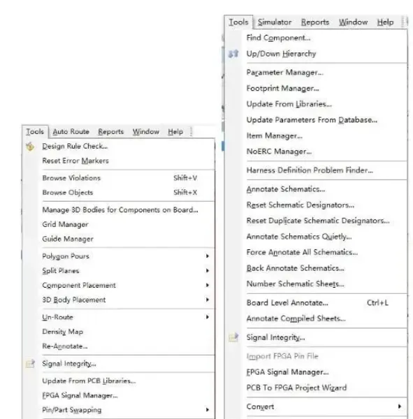
- In the schematic editor, enable cross-probing via the menu: Tools → Cross Select Mode.
- In the PCB editor, enable the corresponding cross-probing option so that selection stays synchronized in both directions.
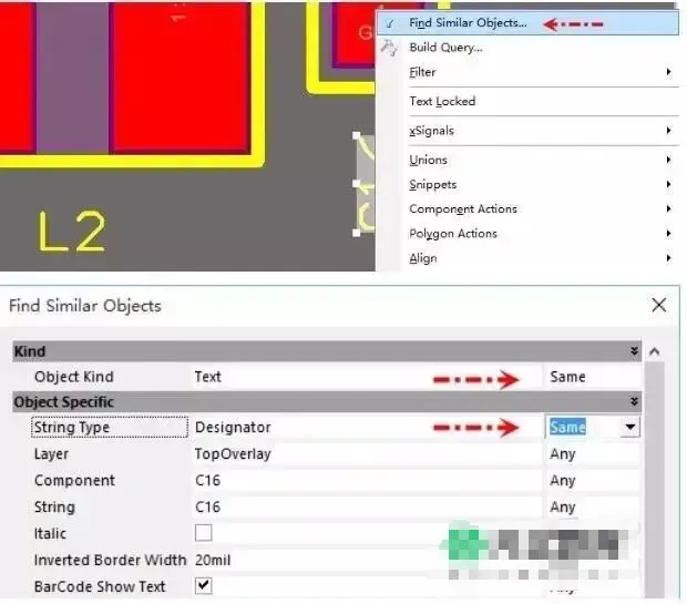
Once active, selecting an individual component or dragging a marquee over multiple symbols on the schematic simultaneously selects and highlights the matching footprints on the PCB. The reverse also applies.
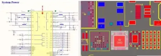
Besides speeding up placement, cross-probing improves design quality. It helps validate that each footprint truly corresponds to its intended symbol, reduces the chance of mixing similar-looking components, and facilitates quick traversal of critical nets for review before routing. It also helps you maintain placement intent: by cross-selecting parts by function, you move logical groups together instead of scattering them across the board.
Usage Tips for Effective Cross-Probing
- Plan selection filters. Limit cross-selection to components (or components and nets) to avoid clutter when box-selecting large areas on the schematic.
- Work with consistent designators and up-to-date ECO synchronization so that cross-references are accurate.
- Use a split view layout—Split Vertical or similar—to keep schematic and PCB visible side-by-side, which makes selection feedback immediate and reduces screen switching.
- Leverage net highlighting during critical block placement. Seeing associated nets helps decide orientation and relative proximity between parts within a block.
Modular Placement: Rapidly Arrange Components in a Defined Area
Even with good cross-probing, an initial pile of footprints can feel chaotic. Modular placement addresses this by arranging a selected set of components into an orderly grid within a defined region. The Arrange Components Inside Area command (often referred to as a rectangular placement box) lets you box-place a group quickly, then refine placements with local adjustments.
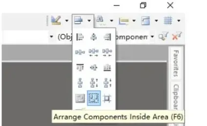
This is especially useful at project start when the board has many unplaced footprints. The goal is to rapidly partition the board into functional regions, place each module within a dedicated area, and maintain clear separation between functions. This approach preserves design intent, simplifies constraint management, and makes subsequent routing more systematic.
Step-by-Step Modular Placement Workflow
- Select a module in the schematic. Using cross-probing, drag-select a functional block such as power regulation, clock generation, or a sensor front end. Confirm the correct symbols are included.
- Confirm the PCB selection. The PCB editor simultaneously highlights the corresponding footprints. Zoom to the selection to verify nothing extra is included and nothing important is missing.
- Arrange within a defined area. Invoke Arrange Components Inside Area and draw or select a rectangle on the board where this module will live. The footprints are automatically arranged within the region in an orderly fashion, using grid spacing and default orientations.
- Refine placement. Manually adjust critical parts—orient connectors and ICs toward known interfaces, place decoupling capacitors as close as practical to power pins, cluster related passives, and ensure thermal and mechanical considerations are met.
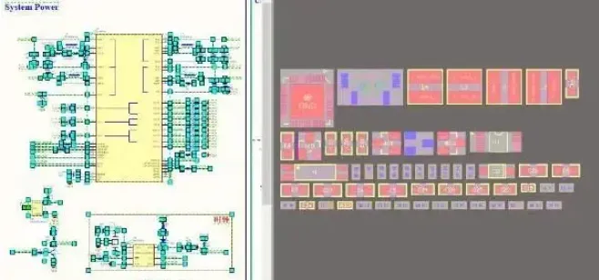
Repeat this process for each functional block. The board quickly evolves from a flat list of footprints into a readable, structured layout with clearly delineated regions. As you refine placement, maintain intent by moving blocks as units when global trade-offs are required.
Practical Guidelines for Modular Placement
- Anchor key parts first. Place connectors, high-pin-count ICs, crystals, inductors, and heat-generating components early, as they constrain orientation and nearby clearances.
- Keep functional proximity. Place related parts close to each other. For example, put power-stage passives near the controller and switch nodes, RF passives near RF IC pins, and decoupling capacitors directly adjacent to power pins.
- Respect placement keepouts and mechanical boundaries. Define and honor areas for mounting holes, shields, thermal pads, and height-restricted zones before arranging blocks.
- Plan routing channels and layer transitions. Leave corridors between blocks for major buses or power rails. Avoid sealing off routes with tightly packed clusters along the same path.
- Consider orientation for assembly and test. Align polar components consistently, avoid hidden test pads under tall parts where possible, and maintain access to debug headers.
- Manage power and thermal paths. Provide room for copper pours, stitching vias, and heat spreading. Don’t pack heat-sensitive components too close to hot devices.
- Use consistent grids and spacing. A consistent snap grid helps maintain even spacing and simplifies later moves and edits.
Why Interactive and Modular Techniques Work Well Together
Interactive cross-probing ensures you are always dealing with the right components by directly binding logical selection to physical placement. Modular arrangement provides an immediate, tidy pre-placement that visually communicates the block’s boundaries and intent. Together, they:
- Reduce placement time by minimizing search and manual alignment efforts.
- Improve placement quality by keeping logical blocks cohesive and well separated.
- Lower rework during routing by anticipating signal flow and interfaces early.
- Support clear communication across the team: a structured board is easier for reviewers, test engineers, and manufacturing partners to understand.
Common Pitfalls and How to Avoid Them
- Overreliance on auto-arrangement. Automated arrangements are a starting point, not a final placement. Always refine critical components for signal integrity, power integrity, thermal, and manufacturability considerations.
- Ignoring decoupling priorities. Even within a neat grid, decouplers need to be as close as practical to their target pins. Break the uniform pattern where necessary to meet electrical requirements.
- Insufficient attention to connectors and external interfaces. Orientation and edge alignment often dictate where blocks can reside. Plan these constraints before locking down module areas.
- Mismatched selection scope. Cross-probing selections that include unintended parts or omit small passives can create incomplete modules. Verify what’s selected on both schematic and PCB before arranging.
- Blocking critical routes. Aesthetically pleasing clusters are not always routable. Leave clearance for differential pairs, high-current paths, and timing-critical nets.
Putting It All Together
A productive placement workflow typically starts with enabling cross-probing in both schematic and PCB. Identify and select a functional module on the schematic, verify the PCB selection, quickly arrange those components inside a chosen area, and then refine with engineering judgment. Progress block by block until the whole board is partitioned and each region is neatly organized. Along the way, maintain awareness of mechanical constraints, thermal paths, and key routing channels to avoid later backtracking.
These techniques scale well. On small designs, they compress placement time and increase clarity. On complex boards, they provide the backbone for a disciplined layout process that preserves logical structure, reduces errors, and shortens iteration cycles. With practice, interactive cross-probing and modular placement become second nature—and the initial placement phase transforms from a bottleneck into a fast, repeatable, and high-quality step of PCB implementation.