Consistent, high-quality PCB design starts with disciplined intake and rigorous mechanical control. A practical checklist prevents avoidable rework, aligns expectations across teams, and ensures that the board you release to manufacturing matches the intended function and mechanical envelope. This checklist consolidates essential items to verify before and during layout, with a focus on design inputs, templates, clock placement, mechanical keep-outs, hole definitions, and protecting the mechanical reference once verified.
1. Verify the Design Input Package Is Complete
Before routing a single trace, confirm that the design package you received is complete and version-aligned. Missing or outdated inputs are a common cause of late-stage redesigns.
- Schematic: Ensure the schematic is the latest approved revision and includes all pages, symbols, and hierarchical blocks. Cross-check that the reference designators match the netlist and BOM.
- Board database file: Verify the board database file (for example, a .brd file) is provided when reusing an existing layout or template, and that it corresponds to the same schematic revision.
- BOM: Confirm that the bill of materials is present and aligns with the schematic. Check for alternates, approved vendors, and any parametric constraints that affect footprint selection or assembly.
- PCB design specification: Review any PCB design notes, constraints, or requirements, including design-rule settings, impedance targets, stack-up constraints, and interface-specific routing constraints (length, skew, topology).
- Change or ECO requests: If this is a revision, ensure formal engineering change orders (ECOs) list all required edits. Verify that the schematic, BOM, and layout directives are synchronized with those changes.
- Standardization requirements: Check corporate or project-standard guidelines that specify layer naming, title blocks, text sizes, naming conventions, datum references, document control, or other standardization constraints.
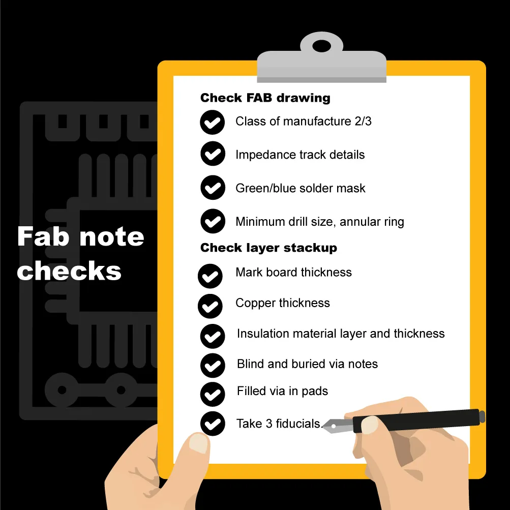
- Manufacturing/process design notes: Review process requirements such as surface finish, solder mask color, silkscreen, via tenting, panelization constraints, assembly notes, and any special fabrication or testing instructions.
Resolve discrepancies upfront. Align version identifiers across the schematic, BOM, constraints, and board database to avoid partial updates. If requirements are ambiguous, escalate early for clarification rather than proceeding with assumptions.
2. Confirm the PCB Template Is the Latest Authorized Version
The template establishes the baseline for stack-up, DRCs, layer naming, keep-outs, documentation layers, and title blocks. Using an outdated template can propagate old rules and documentation errors through the project.
- Layer stack-up and naming: Confirm the stack-up matches the intended impedance and dielectric materials. Ensure layer names and functions align with company standards.
- Design rules: Verify the default constraints (clearances, trace widths, via sizes, differential pair rules, impedance targets, plane clearances) reflect current manufacturing capabilities and project needs.
- Title block and drawing notes: Ensure the title block, drawing numbers, and standard notes are current and conform to the latest document-control procedures.
- Keep-outs and documentation layers: Check that general keep-outs, assembly zones, and documentation layers are present and correctly configured for top and bottom sides.
Once validated, reference this as the only approved template for the project. Clearly document any project-specific deviations and obtain sign-off when needed.
3. Evaluate Clock-Device Placement for Signal Integrity and EMI
Clock oscillators, PLLs, and timing ICs require deliberate placement. Poor placement increases jitter susceptibility, coupling, and radiated emissions.
- Proximity to loads: Place clock sources close to the primary receiver or processor to shorten critical paths, reduce loop area, and simplify controlled-impedance routing.
- Isolation from aggressors: Keep clocks away from switching regulators, high-current power paths, or noisy digital buses. Avoid running clock traces parallel to high dI/dt edges for long distances.
- Ground referencing and shielding: Provide a continuous reference plane beneath clock routes. Where necessary, use ground guard traces or moats to control coupling into adjacent nets.
- Decoupling and return paths: Collocate decoupling capacitors at the clock device with short, low-inductance connections, and ensure clean return paths under the device and routes.
- Differential clocks: For differential clocks, maintain pair coupling with consistent spacing and avoid stubs. Use symmetrical placement and routing to control skew.
Reconfirm the placement strategy during floorplanning. Small adjustments early can significantly improve clock quality and simplify routing.
4. Confirm Positioning Features and Locator Components Are Correct
Positioning features ensure the PCB integrates correctly with enclosures, fixtures, and assembly tooling. Misplaced features can break mechanical fit, test coverage, or assembly alignment.
- Mounting and tooling holes: Verify count, position, diameter, and tolerance of mounting holes and tooling holes. Confirm datum references and coordinate systems match the mechanical drawing.
- Fiducials and alignment marks: Ensure global and local fiducials are included and properly placed per assembly requirements, with adequate solder mask clearance.
- Connector alignment: Check that connectors align with panel cutouts or mating hardware. Confirm keying and polarization features are properly oriented.
- Positioning pegs and locator components: Validate any snap-fit pegs, mechanical locators, or positioning components are placed as specified and use correct hole types.
Engage mechanical engineering early. Validate coordinates against the latest mechanical model, and document any dependencies on enclosure tolerances or gasket compression zones.
5. Ensure Design Notes, Change Requests, and Standardization Requirements Are Unambiguous
Ambiguity in documentation leads to inconsistent interpretation and rework. Create a single source of truth for notes and change directives.
- Clarity and completeness: Write clear, testable statements. Avoid references to undocumented tribal knowledge or "as usual" instructions.
- Revision control: Tag every document and constraint file with revision identifiers. Include change history and ECO references.
- Acceptance criteria: Define what success looks like for controlled impedance, differential skew, timing, and DFM/DFT constraints. If you require fabricator impedance coupons or specific test reports, state them explicitly.
- Consistent terminology: Use common industry terms and internal standards consistently across schematic, layout notes, and fabrication drawings.
When in doubt, add clarifying notes to the fabrication and assembly drawings, and reference governing documents by ID and revision.
6. Reflect Mechanical Keep-Out and No-Routing Zones in the PCB Template
Mechanical drawings often specify areas where components or routing are prohibited due to enclosure constraints, heat sinks, shields, or safety clearances. Ensure these constraints are instantiated in the PCB database.
- Component keep-outs: Transfer top and bottom component keep-outs to the appropriate keep-out layers. Differentiate between strict no-place zones and height-limited zones.
- No-route zones: Add explicit no-route regions for high-risk areas, such as under RF shields, over slots, or near critical mechanical interfaces.
- Assembly and test access: Reserve room for assembly tools, rework access, and test pads. Reflect these as keep-outs if necessary.
- Board edges and breakaways: Define edge clearances for copper and components, including mouse bites or V-grooves, per fabricator guidelines.
Apply DRCs that enforce these zones. Keep-outs should be visible, locked, and part of the documented template so they are not lost in subsequent revisions.
7. Validate Outline Dimensions and Hole Definitions
Compare the PCB outline against the mechanical drawing to verify all dimensions, tolerances, and drill definitions. Incorrect outlines and hole types are a frequent cause of fit failures and assembly issues.
- Dimensions and tolerances: Check the board length, width, contour features, corner radii, and datum references. Ensure dimension chains and tolerances match the mechanical drawing.
- Edge features: Confirm cutouts, slots, chamfers, and notches are present, sized, and constrained as specified. Pay special attention to slots that interface with mating hardware.
- Plated vs. non-plated holes: Explicitly define which holes are plated through (PTH) versus non-plated (NPTH). PTHs are used for vias and through-hole components; NPTHs commonly serve as tooling or mechanical holes. Mismatches can cause plating defects or assembly interference.
- Drill tables and notes: Include a drill table with hole sizes, tolerances, counts, and plating status. Align nomenclature with fabricator expectations to avoid misinterpretation.
Where feasible, include a 3D model export aligned to the same datum references for cross-check by mechanical engineering. This reduces the risk of coordinate system mismatches.
8. Lock the Mechanical Reference After Verification
Once the outline, keep-outs, and critical mechanical features are verified, lock them to prevent accidental edits during layout.
- Lock outline and datum geometry: Protect the board outline, cutouts, and key mechanical features from accidental movement by marking them read-only or locking their layers.
- Lock keep-outs: Prevent modifications to keep-out layers except by designated owners. This reduces the chance of violating mechanical constraints during late-stage routing.
- Protect critical placement: For components tied to the enclosure (connectors, switches, LEDs), lock their placement once agreed with mechanical engineering.
- Use DRCs as guardrails: Enable DRCs that assert violations if mechanical or keep-out rules are breached, and review violations regularly.
Document the lock state and ownership so that intentional changes, when necessary, occur with formal review and updated mechanical sign-off.
Practical Summary
A disciplined PCB design process starts with a complete, traceable design package and a current template. Validate clock placement early for robust SI and EMI behavior. Transfer all mechanical constraints—keep-outs, no-route zones, outline dimensions, and hole definitions—into the PCB database and lock them. Clear documentation, revision control, and enforced DRCs keep the design aligned with both electrical and mechanical intent, reducing risk and accelerating successful release to manufacturing.
Use this checklist as a baseline and adapt it to your organization's standards and product requirements. Small investments in intake rigor and mechanical control pay off in fewer surprises, faster convergence, and more predictable product builds.