Global editing in Altium Designer allows you to modify attributes across the entire board or within a targeted subset of objects in one operation. Typical use cases include resizing silkscreen text and component designators, locking or unlocking components, changing via sizes, adjusting line widths, or toggling visibility. When used with precise selection and filtering, global edits can greatly accelerate PCB design iterations while maintaining control over what is changed.
Ways to Invoke Global Editing
Altium provides several efficient entry points to perform batch edits on similar or selected objects:
- Shift + double-click an object to open context-sensitive controls for that object type and expose a global editing workflow for similar items.
- Select the objects you plan to edit and press F11 to bring up the global editing interface for the current selection.
- Right-click the target object and choose Find Similar Objects. Configure the matching criteria, click OK, and Altium will select all items that match those criteria. You can then apply the desired changes to the entire selection.
In practice, these methods are often used together. For example, you might start with Find Similar Objects to build a precise selection set, then refine or execute the update via the global editing interface.
Example 1: Board-Wide Silkscreen Changes
Silkscreen consistency is important for manufacturing readability and assembly accuracy. Global editing is ideal when you need to standardize text height, width, or font across an entire board or specific layers (e.g., Top Overlay or Bottom Overlay).
Step-by-step Workflow
- Right-click on one of the silkscreen texts you want to change and run Find Similar Objects, as shown in Figure 1. This command lets you build a selection based on object properties of the clicked item.
- In the Find Similar Objects dialog, set properties such as Text and Designator to Same, then click OK. This will select all silkscreen text and component designators that match the chosen criteria. If you need to differentiate between generic text and component designators, ensure you configure criteria accordingly.
- With the matching objects selected, open the global editing panel. Adjust the required attributes. For example, you can standardize text to a height of 0.5 mm and a width of 0.05 mm, then apply the change by clicking OK. Figure 2 illustrates a typical silkscreen global edit session.
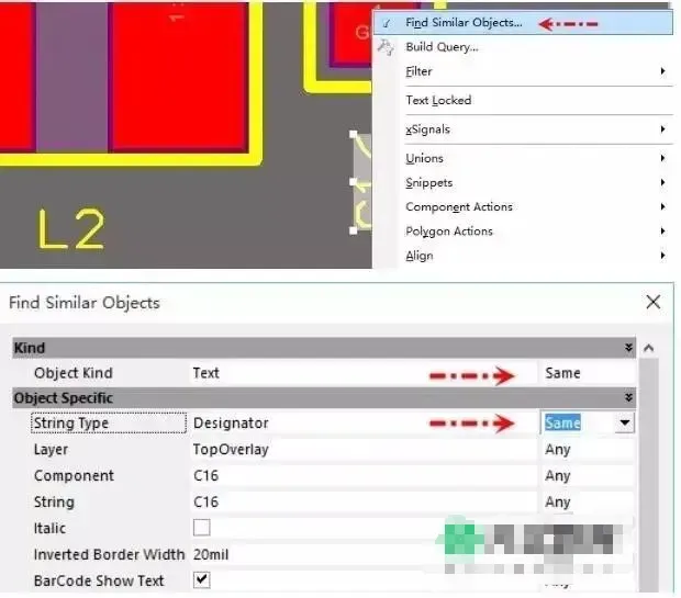
Figure 1 | Configuring Find Similar Objects to build a selection for global edits
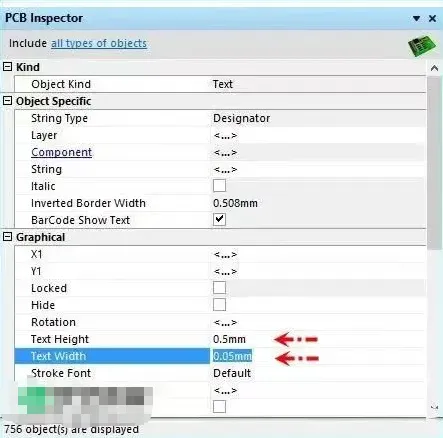
Figure 2 | Batch-editing silkscreen attributes such as text height and width
Practical Notes for Silkscreen Edits
- Text vs Designators: Component designators are a specific text type with extra rules (auto-positioning, visibility per component). If you need to update only designators or only free text, use Find Similar Objects criteria to separate them.
- Layer Scope: Restrict the selection to a single overlay layer if necessary. For example, filter to Top Overlay to avoid unintentionally modifying Bottom Overlay labels.
- Consistency: Use global edits to enforce a consistent silkscreen standard across the project (height, width, stroke, and rotation), improving readability and minimizing DFM issues.
- Selection Confirmation: After Find Similar Objects, visually confirm that only the intended text is highlighted before applying changes.
Example 2: Batch-Edit a Subset of Vias
Another common scenario is adjusting via properties—such as hole size or via diameter—for a specific region or functional area (e.g., a high-current path or a differential pair break-out). Global edits enable you to modify many vias at once while keeping scope limited to a selection window.
Step-by-step Workflow
- Box-select the vias whose attributes you want to change. Restrict the selection to the intended area to avoid touching unrelated vias.
- Press F11 to bring up the global editing interface for the current selection.
- Set the via properties you need to change and apply the updates. Figure 3 shows a typical via batch-edit scenario, where you can adjust parameters such as hole size or overall via diameter for the selected set.
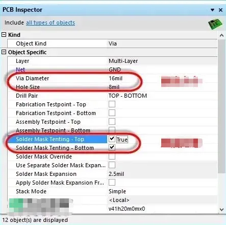
Figure 3 | Global editing of via attributes for a selected subset
Targeted Selection and Filtering Techniques
Effective global edits depend on precise selection. The following techniques help you constrain scope and avoid unintended changes:
- Find Similar Objects: This is often the fastest way to build a selection set based on object properties. For text, you can match on fields such as Text or Designator status. For vias, match on object type and characteristics like hole size or layer span.
- Selection Mode: Decide whether to edit All objects that match the criteria, or only the Selected objects. When working in a dense design, it’s safer to select first and edit only the selection.
- Layer Filtering: Limit selection to a specific layer to prevent multi-layer changes. This is especially important for overlay layers and when changing copper entities.
- Geometric Scope: Use box selection to limit edits to a region. Combine with Find Similar Objects for property matching within that region.
- Locked Objects: If some items are locked (e.g., critical components or reference geometry), ensure your global edit settings respect lock status. Unlock only what you intend to change.
- Preview and Undo: After building the selection, visually scan what is highlighted. Apply changes and immediately verify results. Use Undo to revert if anything unexpected changes.
Common Attributes Suitable for Global Edits
Global editing is most valuable for attributes that must be consistent across many objects. Typical examples include:
- Silkscreen Text: Height, width, font style, rotation, justification, visibility, and layer placement (Top Overlay or Bottom Overlay).
- Component Designators: Font size, width, rotation, visibility, and auto-positioning behavior specific to designator objects.
- Vias: Hole size and via diameter. Global edits are helpful for standardizing via technology across regions, or preparing a design for a specific PCB manufacturing capability.
- Tracks: Line width and net tie-ins for consistent impedance planning or current-carrying requirements in targeted areas.
- Object Lock State: Lock or unlock a set of objects to prevent inadvertent movement during subsequent routing or mechanical adjustments.
Best Practices for Reliable Global Edits
- Define a Clear Scope: Determine whether you are standardizing an entire board, a layer, a functional block, or a routed region. Build your selection accordingly.
- Differentiate Object Types: Treat designators, free text, vias, pads, and tracks as distinct object families. Keep selection criteria specific to the object family you intend to modify.
- Use Units Consistently: Be explicit about units (mm vs mil). For example, when setting text height to 0.5 mm and width to 0.05 mm, verify the unit system to avoid unintended scaling.
- Layer Awareness: Many global edits are layer-sensitive. For silkscreen changes, stick to the correct overlay layer. For copper objects, confirm layer constraints before editing.
- DRC and Fabrication Rules: After batch changes, re-run design rule checks to ensure new sizes, clearances, or text dimensions still comply with manufacturing rules.
- Library and ECO Workflow: If your changes should persist across projects, consider whether they belong in the library. For one-off board-level changes, document the edits to keep your engineering change order (ECO) trail clear.
- Incremental Edits: Apply global changes in small, verifiable steps—e.g., update one layer at a time or one object class at a time—to simplify review and rollback when necessary.
Putting It All Together
Global editing in Altium Designer is a powerful productivity tool for PCB engineers, provided selections are precise and changes are deliberate. Using methods like Shift + double-click, F11 on selected items, and Find Similar Objects, you can rapidly update large sets of objects while maintaining tight control over scope. The silkscreen and via examples illustrate how to configure selection criteria and apply consistent, board-wide standards. By combining careful filtering, layer awareness, and disciplined verification, you can streamline repetitive edits without compromising design integrity or manufacturability.
With practice, these workflows become a natural part of daily PCB design, enabling fast, consistent updates to silkscreen, designators, vias, and other critical attributes across complex boards.