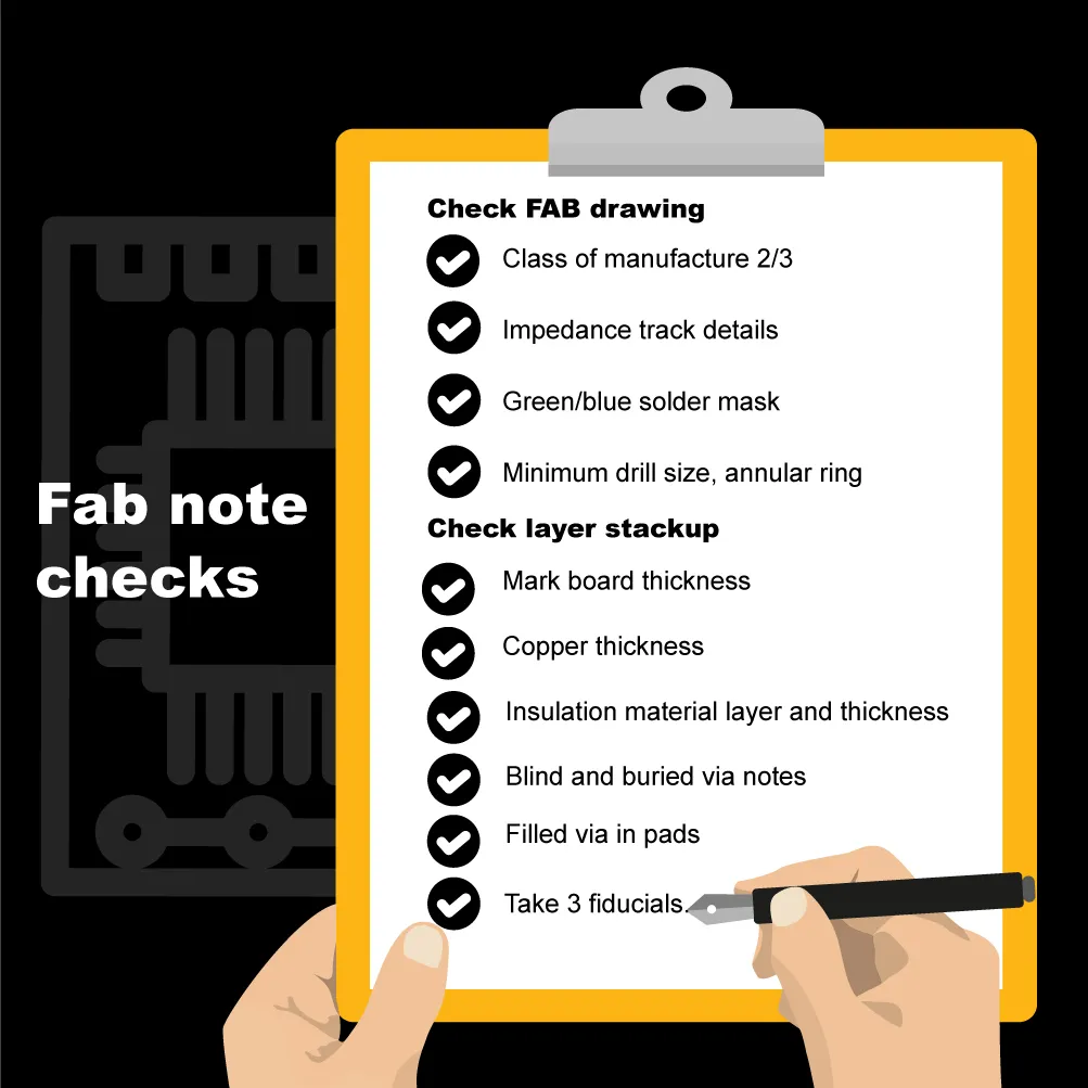
In PCB design, small details are often the difference between a board that builds and performs reliably and one that suffers from rework, yield loss, or field failures. Many recurring issues trace back to how pads are defined, how board outlines and drill data are communicated, how copper pours and solder mask are handled, and how hole sizes are matched to component leads. This practical checklist consolidates common pitfalls and explains the engineering rationale behind each guideline so that designs move smoothly from CAD to fabrication and assembly.

1. Pad Definition and Symbolization
Accurate pad definition is foundational to manufacturability, solderability, and inspection. Misusing primitives or conflating pads and vias can cause incorrect solder mask openings, plating anomalies, and unreliable assembly outcomes.
Use Real SMD Pads, Not Fills, for Surface-Mount Land Patterns
Do not substitute filled shapes or line segments to emulate surface-mount pads. Use proper SMD pads and set the drill to 0 for soldered, non-plated land patterns. SMD pad objects carry the correct behavior in CAM and assembly data: they generate proper solder mask openings, paste apertures, and assembly outlines. In contrast, fills or line segments:
- Do not inherently create solder mask openings, leading to solder mask covering the intended pad.
- Bypass design-rule checks for pad-to-mask and pad-to-copper clearances, increasing the risk of shorts or insufficient solderability.
- Produce ambiguous CAM data for the fabricator, which can result in manual interpretation errors.
Define pad stacks through your EDA tool's pad editor to ensure consistent copper, mask, and paste definitions across all layers and variants.
Do Not Treat Vias and Pads as Interchangeable
Vias and pads serve different purposes and receive different treatments in fabrication. A via is typically a plated through hole used for interlayer connectivity, while a component pad must meet annular ring and solder mask requirements appropriate for soldering. Mislabeling a via as a pad (or vice versa) can cause incorrect plating, mask tenting, or inspection flags. Keep their definitions distinct so the manufacturer can correctly process plating, solder mask, and drill programming.
Keep Silkscreen Off Pads
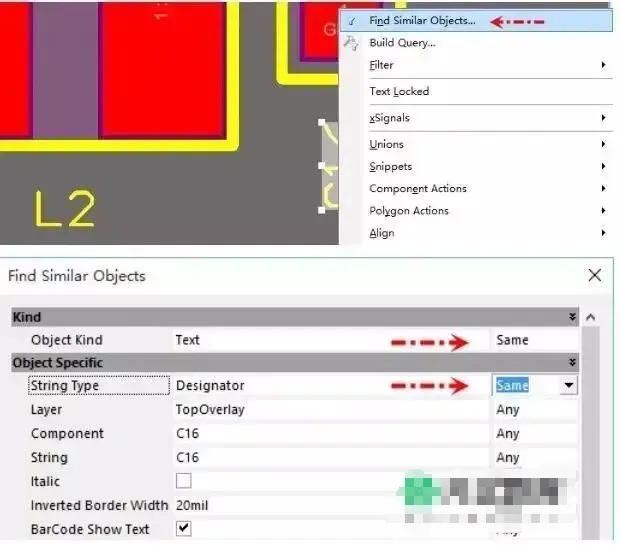
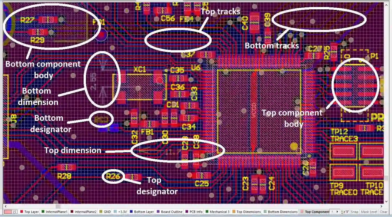
Silkscreen reference designators and polarity marks must not overlap any pads, especially SMD pads and pads on the bottom side. Overprinted silkscreen can contaminate pad surfaces, interfere with solder wetting, and lead to solderability issues or tombstoning. Enforce silkscreen-to-pad clearance rules, and run DRC to catch silkscreen violations on both sides of the board.
2. Board Outline and Drilling Communication
Clear mechanical definitions prevent confusion during CAM, routing, and drilling. Ambiguity here often results in wrong slot widths, edge overcuts, or incorrect plating of holes.
Draw the Board Outline and Special Slots on the Mechanical Layer
Place the board outline and any non-standard features such as irregular slots and rectangular or slotted openings on the Mech1 layer. This keeps the outline separate from copper and mask layers and avoids misinterpretation during CAM. The mechanical layer should include all necessary contours and cutouts so that CNC routing or laser profiling can follow a single, unambiguous path.
Represent Slotted Holes Correctly
When a pad or hole requires a slot, define the drill diameter as the slot width and draw the slot's shape on the Mech1 layer. This communicates both the finished slot width and the exact contour and length. Some CAM flows treat slots as milled features rather than pure drills; providing a clear mechanical outline ensures the slot is manufactured to the correct dimensions and position.
Explicitly Mark Non-Plated Holes
Unless otherwise specified, through-hole pads are typically assumed to be plated through holes (PTH). If a hole must be non-plated (NPTH), mark it explicitly. This distinction matters for:
- Electrical isolation: NPTH features should not have copper connections on any layer.
- Mechanical fit: plating changes hole diameter and wall characteristics, affecting fit and strength.
- Processing: PTH and NPTH holes follow different process steps and tooling approaches.
Clear NPTH notation helps avoid inadvertent copper features and ensures the correct finished hole size and mechanical behavior.
3. Copper Pours: Clearance, Mesh, and Edge Conditions
Copper pours improve current-carrying capacity, thermal performance, and EMI control, but they must be defined with manufacturability in mind. Poorly managed pours can lead to exposed copper, acid traps, or etch defects.
Maintain Sufficient Copper-to-Edge Clearance
Keep large-area copper pours at least 0.5 mm away from the board edge. During routing, chamfering, or depanelization, minimal edge clearance can expose copper, create burrs, or cause copper slivers that lead to shorts or corrosion. A robust edge clearance:
- Prevents copper breakout during panel routing or V-scoring.
- Reduces risk of mechanical damage propagating into the copper.
- Improves reliability in chassis or enclosure contact scenarios.
Respect Minimum Mesh Void Size or Use Solid Copper
For hatched copper pours, ensure the mesh void (the copper-free grid opening) is greater than 15 mil × 15 mil. If you cannot meet this opening size, use a solid copper pour instead. Very small mesh openings are difficult to manufacture consistently and tend to trap etchant or resist, leading to:
- Over-etching or under-etching within the mesh pattern.
- Acid traps and residues that undermine long-term reliability.
- Inconsistent copper widths within the mesh, degrading thermal and electrical performance.
Choosing between mesh and solid pours should consider both thermal relief and manufacturability. When in doubt, coordinate with the fabricator and adhere to their minimum feature and gap requirements.
Solder Mask (Solder Resist) Requirements
Solder mask definitions critically influence solderability, bridging risk, and rework success. Incorrect mask openings can cover pads or leave unintended copper exposed, both of which impair assembly yield.
Ensure Pads Receive Correct Solder Mask Openings
Properly defined pads automatically generate solder mask openings. If you emulate pads with fills or line segments, mask opening rules may not apply, and the solder mask could cover the copper entirely. When unusual pad shapes are required, use pad stacks with defined mask expansion rather than arbitrary shapes. This preserves the intended solderable surface and maintains clearances to adjacent features.
Mark Special No-Mask Areas with Solid Shapes on the Mask Layer
If any region must intentionally remain free of solder mask, draw a solid keepout shape on the appropriate mask layer. This explicit definition ensures that the CAM output removes solder mask in that region, preventing misinterpretation and rework during manufacturing.
Tent Vias Adjacent to BGA Pads on the Component Side
For vias placed near BGA pads on the component side, cover the via with solder mask (tented via). Tenting reduces the risk of solder wicking into vias during reflow, which can otherwise deplete solder from the BGA ball and cause opens or weak joints. It also helps prevent solder bridging between adjacent features and minimizes flux residue accumulation near dense BGA arrays.
5. Component Leads and Hole Size Planning
Through-hole design requires careful coordination of component lead dimensions, drill sizes, plating, and annular rings. Poor sizing or pad definition can cause tight fits, lead damage, or inadequate solder fillets.
Accommodate Square Leads by the Diagonal
For square-section leads with a side length less than 3 mm, size the hole slightly larger than the lead's diagonal. This ensures the lead can pass through without shaving or deforming, and maintains suitable clearance for solder flow. Remember that plated hole walls reduce the effective finished hole diameter, so set hole sizes based on finished dimensions and process capability rather than nominal drill sizes.
Panelizing Multiple Boards in a Single File
If multiple different boards are drawn in a single project, define a distinct border for each board and maintain at least 100 mil spacing between them. Adequate spacing provides room for routing tabs, breakaway features, or tool paths during panelization and depanelization. It also prevents copper features from different designs from unintentionally interacting or violating spacing rules when panelized.
Pad Diameter Relative to Hole Size
Set the pad diameter to be at least the hole diameter plus 18 mil. This margin provides a robust annular ring around the hole, accommodating drill wander, layer registration tolerances, and plating variations. A sufficient annular ring:
- Improves mechanical strength of the pad-to-hole interface.
- Reduces the risk of breakout or exposed substrate at the pad edge.
- Increases reliability under thermal cycling and mechanical stress.
Use your EDA tool's pad stack manager to embed these relationships so that any changes in hole size automatically update pad diameters, maintaining consistent annular ring targets across the design.
Putting It All Together: DFM-Oriented Workflows
A DFM-aware PCB design process captures intent unambiguously and aligns with manufacturing practices. Consider embedding the following practices in your workflow:
- Use the correct primitives for each feature: SMD pads for surface-mount, through-hole pads for components, vias for interlayer connections, and mechanical layers for outlines and slots.
- Lock in pad stack definitions that include copper, mask, and paste layers, along with consistent annular ring and clearance targets.
- Apply global rules for silkscreen-to-pad clearance, copper-to-board-edge clearance, and mask expansion, and verify enforcement with DRC.
- Clearly distinguish PTH and NPTH holes, and document slot widths and contours on the mechanical layer.
- Coordinate copper pours with fabrication limits: maintain minimum void sizes in meshes, or switch to solid pours when meshes become too fine.
- Use tented vias in sensitive regions such as under BGA packages to contain solder and reduce bridging risk.
- Plan hole sizes against finished dimensions and anticipate plating effects on hole diameter.
Consistency across these elements reduces back-and-forth with the fabricator, shortens lead times, and raises first-pass yield. By formalizing these rules into your design templates and checklists, every new project benefits from the same robust manufacturability baseline.
Attention to these details not only prevents re-spins but also strengthens product reliability in the field. When in doubt, consult with your PCB fabricator about their specific process capabilities and preferred data conventions, and reflect their guidance in your design rules and documentation.