When building a PCB layout, it's easy to end up with components that look slightly skewed, unevenly spaced, or just visually untidy. Manually nudging every footprint into place wastes time and often introduces inconsistencies. Altium Designer provides built-in alignment and distribution tools that align components precisely and space them evenly with a few keystrokes. With these tools, arranging components can feel as straightforward as snapping building blocks into place.
If you have ever found that device placement looks off, spacing feels inconsistent, or alignment requires too much dragging and zooming, the alignment hotkeys can dramatically speed up your workflow and produce a cleaner, more professional layout.
One-Click Alignment and Even Distribution
Most PCB tools rely on grid snapping for placement, which helps but doesn't guarantee uniform alignment or consistent spacing across a selection. Altium Designer goes further with an intelligent alignment and distribution feature set. You can align a group of components to a common edge or centerline, and evenly distribute them horizontally or vertically. These commands operate on the selected objects and apply immediately, reducing the need for incremental manual adjustments.
Common use cases include aligning rows of connectors to a precise edge, aligning decoupling capacitors relative to an IC, or distributing LEDs evenly along a panel edge. Whether you need left, right, top, or bottom alignment, or want to spread parts uniformly across a span, these actions can be performed in one step.
Shortcut AA: A Productivity Booster
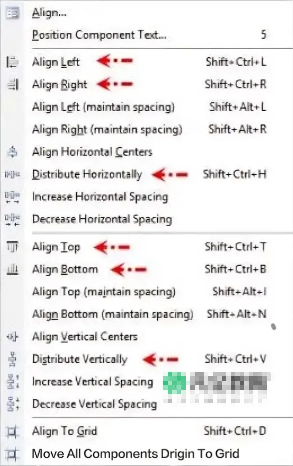
Altium Designer exposes a concise keyboard-driven workflow for alignment. After selecting the components you want to organize, use the AA key sequence to invoke alignment functionality, followed by specific hotkeys for the desired operation. Instead of dragging items one by one, the hotkeys apply consistent, predictable alignment across the entire selection.
Here is a quick reference for commonly used alignment hotkeys:
| Function | Hotkey | Result |
|---|---|---|
| Align left | AL | Align all selected components to the leftmost edge |
| Align right | AR | Align all selected components to the rightmost edge |
| Align top | AT | Align all selected components to the top edge |
| Align bottom | AB | Align all selected components to the bottom edge |
| Distribute horizontally | AD | Evenly distribute selection in the horizontal direction |
| Distribute vertically | AS | Evenly distribute selection in the vertical direction |
With these shortcuts, you no longer need to manually drag each footprint to line them up. The result is a faster, more consistent layout process with a cleaner outcome.
Why Alignment Matters in PCB Design
Alignment and uniform spacing are not just about aesthetics. They also contribute directly to design quality, manufacturability, and routing efficiency:
- Routing efficiency: Well-aligned components shorten routing paths and reduce congested areas. Straight, parallel runs for buses and connectors are easier to route, minimize crossovers, and reduce the need for meanders later.
- Signal integrity: Consistent placement supports cleaner routing topologies for high-speed signals. Regular, parallel routes help maintain consistent impedance environments and reduce the chance of unnecessary stubs or abrupt jogs.
- Power delivery and decoupling: Aligning decoupling capacitors around a device can help enforce consistent, short return paths and make placement more systematic across similar ICs.
- Manufacturability and assembly: Uniform spacing and alignment improve pick-and-place predictability and help ensure sufficient clearances for inspection, rework, and automated optical inspection.
- Mechanical and human factors: Aligned connectors and indicators improve product usability and fit in enclosures. Consistent orientation and spacing for LEDs and switches improve readability and user interaction.
- Clarity and consistency: A tidy layout is easier to review, maintain, and reuse. Alignment reduces ambiguity and speeds up peer reviews or design audits.
Practical Workflow and Tips
Selecting and Anchoring Objects
Start by selecting the objects to be aligned or distributed. You can use box selection, multi-select with modifier keys, or selection filters to target specific object types (such as components only). Most alignment operations respect the bounding boxes of the selected items. Typically, the align operation references the extreme item in the group (e.g., the leftmost item for Align Left) and moves others to that reference. If you want a specific item to act as the anchor, include it in the selection and ensure it sits at the intended boundary.
When arranging components relative to a known datum—like a board edge or mechanical feature—consider first snapping the anchor component to that datum using your grid or snapping settings. Then, run the alignment on the rest of the selection for a precise result tied to that reference.
Horizontal and Vertical Distribution
Distribution spreads selected components evenly along one axis. For example, distribute horizontally to place equal spacing between connectors along an edge, or distribute vertically to align LEDs or test points along a consistent column. Distribution is particularly useful when the outermost items are correctly placed and you need to fill the span uniformly without manual measurement.
Keep in mind that distribution typically uses the overall span of the selection's bounding box. If the bounding box includes outliers or items not intended to define the span, refine the selection to include only the intended items and ensure the endpoints are fixed in place before distributing the rest.
Aligning to Component Origins vs Bounding Boxes
Alignment can be based on bounding boxes, which reference the outer edges of each selected object. This is usually desirable for mechanical consistency. However, it's helpful to remember that component footprints also have placement origins. If your workflow relies on precise origin-based alignment—for instance, aligning multiple identical modules by their origins—make sure your selection and snapping mode reflect that intent. Where necessary, adjust the reference item's origin or use mechanical reference geometry to ensure consistent results.
Avoiding Common Pitfalls
- Clearance constraints: After alignment, verify component-to-component clearances still meet design rules. Tight clusters may violate minimum spacing even if visually aligned, especially for tall components or those requiring service access.
- Net and polarity orientation: Aligning can inadvertently flip or rotate components out of their intended orientation if not constrained. Ensure that polarities, pin 1 orientation, or keyed connectors remain correct after movement.
- Anchoring unexpected items: If an unintended object is part of the selection, it can redefine the bounding reference and produce an undesired result. Use selection filters or carefully review the selection before running commands.
- Distribution span: The distribution uses the outermost selected items as boundaries. If those endpoints are not where you want the span to begin and end, reposition them first, then distribute the remainder.
Integrating Alignment with Routing and Rules
Alignment is most effective when paired with thoughtful rule configurations and routing strategies. Set appropriate grids and snapping to speed up precise placement relative to board edges and mechanical features. Keep-out regions, component clearance rules, and room definitions help ensure that automated moves respect constraints. After alignment, you can apply routing optimizations more consistently—for example, creating uniform bus routes or symmetrical differential pair entry points.
For repetitive structures—such as multiple identical channels—consider aligning one channel perfectly, then using copy-and-place techniques to replicate the entire group. This preserves relative alignment and spacing, yielding consistent routing patterns across channels.
Conclusion
Clean alignment elevates both the appearance and functionality of a PCB layout. Altium Designer's alignment and distribution hotkeys deliver fast, repeatable results without tedious manual nudging. With a few keystrokes—AL, AR, AT, AB for edge alignment and AD, AS for equal spacing—you can bring order to component placement, streamline routing, and improve manufacturability. Good alignment is not cosmetic; it's a practical step that enhances design quality and speeds up the entire layout process.
Align precisely, distribute evenly, and let the layout workflow become both efficient and visually clear.