After the schematic is finished and components are imported into the PCB, you may face a tangle of ratlines and not know which part to move first. Some place the largest chip in the center, some line components along the board edge, and others fill any available space. A practical starting point is to first distinguish which positions must not be moved, which components must be adjacent, and which areas must be kept clear. Placement is not merely arranging components neatly; it anticipates how the circuit will be routed, how the board will be assembled, and how it will be accessed during debugging. For a first low-voltage, low-density board, perform an initial placement pass using the four position types below before broad routing.
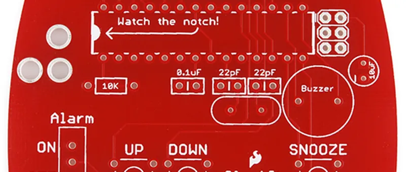
Figure 1 | Partial bare-board view of the clock circuit; the positions of the button and buzzer influence the placement of nearby components.
01 | Lock down positions that must not be moved
Start with the board outline and mechanical constraints, then consider component sizes. Mounting holes, buttons that must align with the enclosure, display windows, and external connectors are typically decided earlier than the main controller's location. Connectors also require clearance for mating and unmating — you can't rely solely on whether the solder pads fit on the PCB. If dimensions are not confirmed, mark them as "to be confirmed" rather than treating guesses as fixed constraints.
Write three simple notes next to the board outline: where the board will be installed, from which side the user operates it, and where cables enter and exit. Even for a practice board, set these boundaries deliberately. Otherwise a layout that appears compact may later force you to move half the board because of a connector orientation. If you have the actual connector, check the mechanical drawing and mating direction; don't estimate from product photos. Always confirm size information against component mechanical drawings and enclosure documentation.
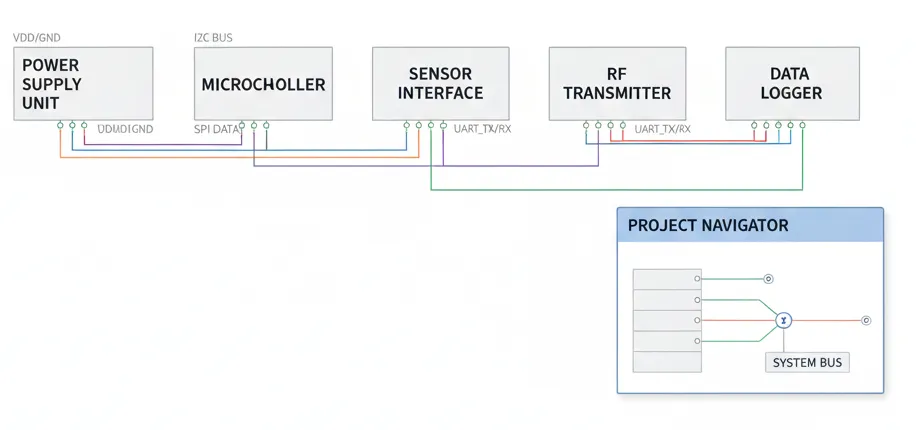
Figure 2 shows components just imported. Having all components present does not mean placement has started; the actual first step is to incorporate mechanical positions and functional requirements. A practice board's outline can iterate, but when a product already has an enclosure you cannot change the board outline simply to suit component placement.
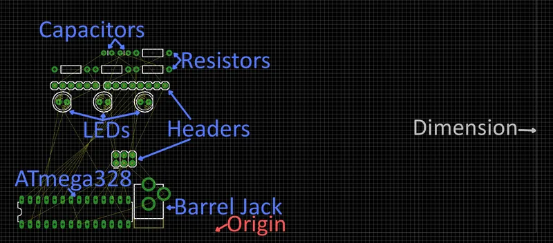
Figure 2 | Components just imported into the board outline; ratlines show electrical connections yet to be routed.
02 | Arrange functional blocks along their connection relationships
Divide the schematic into readable functional sections—e.g., power input, main controller, sensor interfaces, display or LEDs. Ask "who hands a signal to whom" and use that to determine proximity. This produces not isolated chips but connection paths with clear start and end points.
The main controller does not have to be at the geometric center. If most interfaces are on one side, place the controller toward that side to simplify routing. If there are sensitive analog inputs, consider their relationship with noisy circuits. What is "appropriate" depends on the actual circuit — there's no universal millimeter spacing rule.
Crossing ratlines can suggest awkward placement, but they shouldn't be the only judgment. Identify critical connections first, then try rotating or moving whole functional blocks. Don't sacrifice confirmed interface positions or local component requirements just to minimize every ratline length.
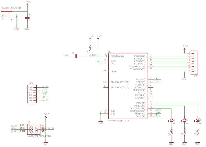
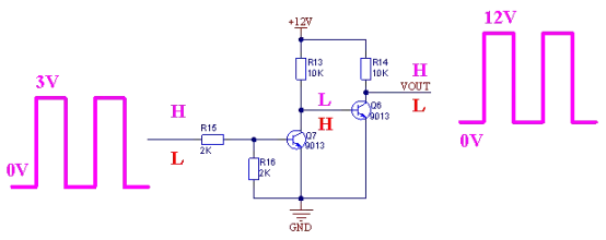
Figure 3 | Example schematic used to identify the main controller, interfaces, LEDs, and other functional blocks.
03 | Small components also have their fixed "partners"
Decoupling capacitors, clock-related parts, feedback resistors, and similar small parts are not just filler. Decoupling capacitors supply local current for fast transients near a chip; if they are far from the power pins the connection path can undermine their effectiveness. Check the chip datasheet for recommended placement before deciding component locations.
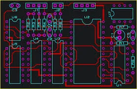
Figure 4 shows components arranged according to function, with controller, connectors, LEDs, and resistors grouped by relationship. When reading the figure, focus on which component serves which device rather than copying absolute coordinates. This simple example uses through-hole parts and should not be taken as a standard layout for high-speed or high-density products.
A practical move is to circle these local groups on the schematic and try to move them together during placement. If the main IC position changes, re-evaluate these groups rather than moving the controller and leaving peripherals in place.
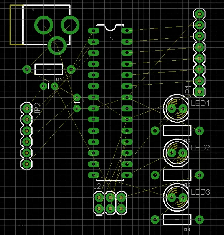
Figure 4 | Component placement arranged by functional relationships; the MCU's surrounding components are grouped logically rather than placed arbitrarily.
04 | Reserve access for routing, soldering, and debugging
It's common to fill the board and only then discover that traces have nowhere to go, forcing a rework. Before routing, walk a few critical connections and check whether any channel is blocked by components, whether interfaces can be routed out, and whether power and ground can be connected with reasonable spacing. Blank areas are not necessarily wasted space; they may be required to complete the design.
Simulate actual use: can the programming or debug cable mate, are common probe points accessible, and are polarity marks clear? Areas that require hand soldering or rework need operator access based on component package and assembly method. For production, confirm placement and clearances with assembly and test engineers—don't assume a universal pad or spacing will cover every process need.
Figure 5 shows the same design after routing. It reminds us that placement's value is ultimately judged by whether the connections can be made successfully. Basic manufacturability checks still matter, but this initial pass aims to give placement a rationale and a direction for further iteration rather than solving every process detail.
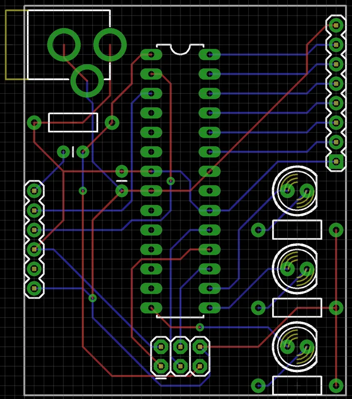
Figure 5 | Same example board after routing; this lets you review which placement choices facilitated the connections.
Place constraint-driven items first, then pursue compactness. Next time you open a PCB, try marking fixed positions, functional blocks, local component partners, and reserved areas. Clarify the most uncertain dimensions before routing. This sequence is a basic checklist for beginners and does not replace device- or product-specific design requirements. For your current board, what dictates placement first: external interfaces, mechanical mounting, or a critical signal path?