Analog data is continuous and originates from sensors measuring real-world variables such as temperature and pressure, as well as audio and video in telephony, radio, and broadcast applications. Digital data, by contrast, consists of discrete values obtained by quantizing analog signals and encoding them in formats such as binary for characters, graphics, audio, and video in computing systems.
Digital circuits have defined noise margins and are inherently tolerant to a certain level of noise without loss of functionality. Analog circuits are far less forgiving: noise directly degrades signal fidelity, reducing performance and, in severe cases, driving the analog subsystem out of specification. In mixed-signal designs, shared current loops between digital and analog domains create efficient pathways for digital noise to couple into sensitive analog circuits. Without deliberate partitioning, routing, and grounding strategy, this coupling can cause severe electromagnetic interference (EMI) and functional failures in the analog section.
Common Interference Mechanisms in Mixed-Signal Systems
1. Coupling from Digital Signal Traces into Analog Circuits
If a design lacks explicit partitioning and routing separation, digital signals may run over, under, or adjacent to analog signal paths (and vice versa). The resulting coupling—often dominated by inductive mechanisms when fast-edged digital currents create changing magnetic fields—injects noise into the analog nodes and degrades their signal-to-noise ratio. To mitigate this:
- Place and route digital and analog subsystems in clearly defined regions. Avoid interleaving to keep high dI/dt digital currents away from analog traces.
- Provide a solid, continuous reference plane under both regions so return currents follow the shortest path directly under their aggressors, minimizing loop area and magnetic coupling.
- When crossing between regions is unavoidable (for example, an ADC interface), route crossing signals over an uninterrupted ground plane, and keep them as short and direct as possible.
- Maintain spacing between fast digital traces (clocks, high-frequency buses) and sensitive analog nodes, and avoid long parallel runs.
2. Interference via Digital Power and Ground into Analog Circuits
Mixed-signal ICs often maintain internal separation between their analog and digital grounds and supplies. However, at the system level, all subsystems must reference a common ground to operate coherently. Any external impedance tied to the digital ground can, through parasitic capacitances, couple digital noise into the IC’s internal analog circuits. Similarly, noise on digital power can couple into the analog section. The result is ground bounce, reference instability, and spurious tones or noise floor elevation in analog outputs.
Two practical grounding strategies are commonly applied to control this coupling:
2.1 Single-Point or Multi-Point Ground Connections
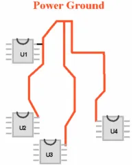
One approach separates the analog ground (AGND) and digital ground (DGND) regions and rejoins them at a carefully chosen location with a low-impedance “ground bridge.” The objective is to control the location of shared return currents so they do not flow through sensitive analog ground areas.
Depending on the system topology, use:
- Single-point grounding when there is a single connection between analog and digital domains—for example, a system with one ADC or one DAC where the primary interaction is localized. The single tie forces return currents to rejoin at the designated point.
- Multi-point grounding when multiple ADCs/DACs or multiple analog-digital interfaces exist. In such cases, controlled multiple ties reduce the impedance between domains and prevent excessive return detours caused by a single distant connection.
Important constraints accompany split-ground strategies. Crossing signals must never traverse a split in the reference plane; otherwise, their return current detours around the split, dramatically enlarging loop area and radiated emissions. If a split must exist, locate the bridge directly under the crossing interface so the return path remains short and well-defined.
2.2 Zoning Without Splitting the Ground Plane
A second approach—which is increasingly favored in vendor reference designs for ADCs and DACs—is to maintain a unified, low-impedance ground plane while strictly zoning placement: analog components remain in the analog region and digital components in the digital region. The ground plane itself is not physically split.
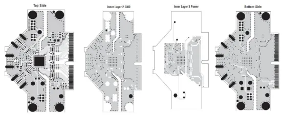
This method offers several advantages:
- It ensures a low-impedance connection between AGND and DGND pins, as many IC vendors recommend. Short, direct connections minimize reference noise.
- It avoids creating loop or dipole antennas that can result from poorly executed ground splits, improving EMC performance.
- It preserves well-controlled return paths for signals that must cross between domains, since the return current remains directly beneath the aggressor on the continuous plane.
In practice, zoning without splitting simplifies routing, reduces the risk of return-path discontinuities, and still delivers effective isolation when combined with disciplined placement and decoupling.
3. Crosstalk Between Similar Analog Subcircuits
Parallel analog modules can interfere with each other through shared ground or power rails. To reduce mutual coupling:
- Use single-point connections for module grounds or, where justified, isolate module grounds so sensitive returns do not mingle. Ensure any isolation choice preserves a controlled return path back to the main ground reference.
- Isolate module power feeds using ferrite beads and place local decoupling capacitors close to each module. The bead impedes high-frequency noise propagation between modules while the local decoupling sustains the module’s instantaneous current demands.
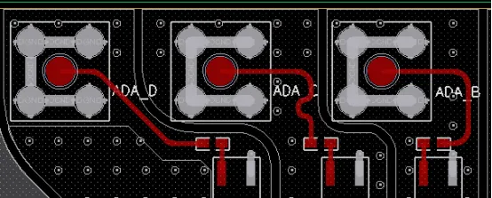
When selecting ferrite beads, ensure their impedance peaks across the dominant noise frequency range of your system, and place them to avoid long stubs. Always maintain a solid ground return to prevent inadvertently introducing ground loops or excessive ground impedance.
4. Transmit-to-Receive (Tx-to-Rx) Interference Within Analog Sections
In many communication systems, transmit and receive circuits operate side-by-side. Transmit signals are typically orders of magnitude stronger than receive signals. Without isolation, the powerful Tx energy can couple into the sensitive Rx path, overwhelming weak inputs and desensitizing the receiver.
Mitigation practices include:
- Physical separation between Tx and Rx paths to reduce magnetic and electric field coupling.
- Shielding using continuous ground planes and, where needed, grounded guard structures that confine fields. Stitch ground vias along shield edges to maintain continuity and reduce slot antenna effects.
- Dedicated power filtering for Tx and Rx circuits so high level transmit activity does not modulate the receive supply or reference.
Practical Layout and Power Integrity Guidelines for Mixed-Signal PCBs
Beyond the specific mechanisms above, robust mixed-signal performance hinges on controlling return paths, managing high di/dt currents, and preserving low-impedance references. The following practices build on the same principles discussed earlier and help translate them into consistent PCB outcomes.
Layer Stackup and Reference Planes
- Use continuous ground planes adjacent to signal layers to provide low-inductance return paths. Avoid plane discontinuities—slots, splits, or narrow neck-downs—under critical signals.
- When routing signals on orthogonal layers (for example, horizontal on one layer and vertical on another), the orthogonality helps reduce broadside coupling between layers, particularly for long runs.
- Place the most sensitive analog traces over the quietest parts of the ground plane and away from digital clocks and fast switching nodes.
Decoupling and Local Regulation
- Decouple both analog and digital supply pins at each device with short, low-inductance connections to the ground plane. Use a mix of capacitors selected to cover the relevant frequency range of the device’s transient currents.
- When an IC provides separate AGND and DGND pins, follow the vendor recommendation for connecting them—often a short, direct tie at the device—while ensuring the PCB ground beneath remains continuous.
- Where feasible, feed analog sections through filtered power nodes (for example, using ferrite beads), and place local LDOs for especially sensitive references. Keep the filter path tight and avoid introducing long, resonant stubs.
Signal Crossings Between Domains
- When a digital signal must enter an analog region (for example, the digital interface to an ADC), route it over an uninterrupted ground plane. Minimize its loop area by keeping the trace close to the plane and avoiding unnecessary vias.
- Do not route crossing signals over ground splits or discontinuities. If the design uses a ground bridge, align the crossing directly above it so the return current path is as short and direct as possible.
- Keep clock lines and other high-frequency digital signals as far as practical from analog inputs, references, and outputs. If necessary, add ground shields between aggressor and victim routes, ensuring the shield is well stitched to ground.
Placement and Zoning Discipline
- Group components by function and signal bandwidth: high-speed digital, low-level analog inputs, precision references, and power regulation should each be clustered and oriented to minimize cross-coupling.
- Align interfaces at the boundary between zones to avoid long traversals across domains. Place ADCs and DACs at the edge between analog and digital regions so analog signals remain in the analog zone and digital signals in the digital zone as much as possible.
Verification and Iteration
- Review current return paths explicitly during layout. Traces are only half of the circuit; returns determine EMI and crosstalk susceptibility.
- During bring-up, measure noise at critical analog nodes and power rails under representative digital activity. Look for correlations between digital events (such as clock bursts) and analog performance deviations. Use this feedback to refine decoupling networks, bead placement, and zoning in subsequent revisions.
Ultimately, mixed-signal PCB design succeeds when the analog and digital domains are treated as coupled systems rather than independent subsystems. By controlling return paths, defining where domains connect, and maintaining continuous, low-impedance references, designers can minimize interference and deliver both robust digital functionality and high analog fidelity.