Many schematics show two small capacitors tied between VCC and ground, often 0.1 μF and 0.01 μF. They are not redundant parts. Each addresses a different piece of the same engineering problem: keeping the supply rail quiet and stable across a wide frequency range while isolating interacting circuits. This article clarifies the meanings of bypass and decoupling, explains where each capacitor belongs, and shows why two values are commonly used in parallel.
Bypass vs. Decoupling: What the Terms Mean in Circuits
In everyday English, "bypass" means taking a shortcut. The same idea applies in circuits: a bypass path provides an alternate, lower-impedance route for unwanted AC content so it does not pass through the sensitive load. A bypass capacitor presents a low-impedance path to ground for high-frequency noise on a power rail, diverting it away from the IC's pins.
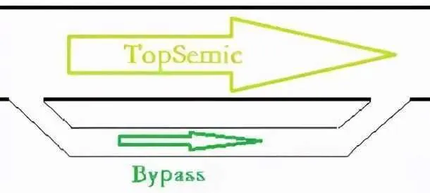
"Coupling" refers to one system's signals inducing activity in another system. Power rails are a common coupling path: switching transients from one IC can modulate the shared supply and disturb other devices. "Decoupling" reduces this coupling by providing a local energy reservoir at each device so its current transients do not propagate onto the rail.
Where the Two Capacitors Fit in a Simple Power–IC Circuit
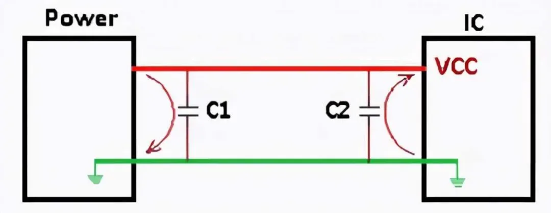
The figure below shows a DC source powering an IC with two capacitors on the rail. One capacitor is placed close to the source (bypass), and the other is placed close to the IC pin (decoupling). This placement reflects two complementary goals:
- Shunt high-frequency noise on the rail to ground before it reaches the load (bypass).
- Keep the IC's own switching transients local and off the rail (decoupling).
Bypass: Diverting High-Frequency Noise on the Supply
High-frequency disturbances can ride on the power rail, whether they originate in upstream converters, other loads sharing the rail, or radiated coupling. If this noise reaches the IC, it can disturb thresholds, increase jitter, and degrade signal integrity.
Placing a capacitor near the source node of the rail provides a low-impedance path to ground for the high-frequency portion of that noise. Because a capacitor blocks DC but looks like a low impedance at sufficiently high frequencies, the unwanted AC content "bypasses" the IC and returns to ground through the capacitor. This is the role of the bypass capacitor.
Decoupling: Providing Local Transient Current for the IC
Most ICs draw rapidly changing current as internal gates switch or as clocks start, stop, and change frequency. These di/dt events cause voltage droop and ringing if the supply path's inductance and resistance are significant. If these transients propagate back onto the rail, they can modulate the supply seen by other loads or excite the upstream regulator.
Placing a capacitor directly at the IC's VCC pin provides a local charge reservoir that can source current for fast transients and sink returning charge. This keeps the voltage at the IC pins stable during switching events, while reducing the amount of disturbance that reaches the wider power distribution network (PDN). In this role, the capacitor decouples the IC from the rest of the system.
Why Two Capacitors Instead of One?
A common question is: if a 0.1 μF capacitor already bypasses and decouples, isn't adding a 0.01 μF capacitor wasteful? The answer lies in real-world component behavior versus frequency.
Capacitive Reactance and Frequency
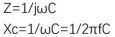
The magnitude of a capacitor's reactance is inversely proportional to frequency and capacitance value:
Xc = 1/(2πfC)
At a first glance, a larger capacitance always seems better because it yields a lower Xc at the same frequency. But real capacitors have parasitics—equivalent series resistance (ESR) and equivalent series inductance (ESL)—that fundamentally change their impedance versus frequency curve.
ESL, ESR, and Self-Resonant Frequency (SRF)
Every MLCC exhibits a self-resonant frequency (SRF) set by its nominal capacitance and ESL. Below SRF, the capacitor behaves capacitively and its impedance falls with frequency. At SRF, impedance reaches a minimum. Above SRF, ESL dominates and the component behaves inductively, so its impedance rises with frequency.
Two implications follow:
- A single capacitor cannot maintain low impedance across a wide frequency span. It is only strongly effective around and below its SRF.
- Higher-value capacitors tend to have lower SRF. They are useful at lower-to-mid frequencies but become inductive at higher frequencies, where very small capacitors still behave capacitively.
Extending the Effective Bandwidth with Parallel Values
Paralleling different capacitance values broadens the frequency range over which the PDN presents a low impedance:
- The 0.1 μF capacitor lowers impedance in the mid-frequency region around its SRF, supplying moderate-speed transients and shunting noise in that band.
- The 0.01 μF capacitor, with a higher SRF, keeps impedance low at higher frequencies where the 0.1 μF device has already turned inductive, capturing very fast edges and high-frequency noise.
In other words, the two capacitors complement each other spectrally. Together, they maintain a low-impedance path over a wider bandwidth than either one alone. From a time-domain perspective, this combination reduces both the amplitude and duration of supply droop and ringing caused by rapid load-step currents.
What About Anti-Resonance?
When multiple PCB capacitors are placed in parallel, their ESLs and ESRs can interact to create anti-resonance peaks—narrow frequency bands where the combined impedance briefly rises. In many practical layouts, the inherent ESR of small ceramic capacitors and the inductance of mounting interconnects provide enough damping to keep peaks modest. Sensible layout techniques (short connections, separate low-inductance vias to power and ground planes, and tight loops) reduce ESL and smooth the impedance profile. The result is still a much lower net impedance across most of the band compared with a single capacitor.
Placement and Layout: Turning Theory into Measured Performance
Parasitics are dominated not just by the capacitor itself but by how it is mounted. To make the two-capacitor strategy effective:
- Place the decoupling capacitor as close as physically possible to the IC power and ground pins. Short, wide connections and direct vias into the planes minimize loop inductance, improving the high-frequency effectiveness.
- Keep the return path compact. The physical loop formed by the IC pin, capacitor, and ground return should be as small as possible to reduce ESL and radiated coupling.
- Place the bypass capacitor at a strategic point on the rail where incoming high-frequency noise can be shunted to ground without traversing sensitive loads. In systems with a central regulator feeding multiple ICs, additional bulk and mid-band capacitors near the source help keep the upstream impedance low.
- Use separate vias for the capacitor's power and ground terminals when connecting to planes. Shared vias increase shared inductance and degrade high-frequency performance.
- Avoid long stubs or thin serpentine routes between the capacitor and the pin they support. Route directly and keep interconnect geometry compact.
Putting It All Together
Bypass and decoupling address two sides of the same goal: prevent high-frequency disturbances from traveling where they can do harm and ensure local charge is available where it is needed. In practice:
- The bypass capacitor on the rail gives high-frequency noise a low-impedance "shortcut" back to ground so it does not cross the sensitive load.
- The decoupling capacitor at the IC pin supplies and absorbs switching current locally, reducing supply ripple at the device and limiting the disturbance reflected onto the broader PDN.
- Using two different values—such as 0.1 μF and 0.01 μF—extends the bandwidth over which the supply presents low impedance. The higher value addresses mid-band transients; the smaller value remains effective deeper into the high-frequency region where the larger one has become inductive.
The result is improved supply stability, reduced coupling between circuits that share a rail, and better signal integrity. While the exact values and quantities should be guided by the device's current spectrum and the PDN's impedance targets, the 0.1 μF + 0.01 μF pairing remains a pragmatic, effective starting point. Its effectiveness, however, hinges on good PCB implementation. Capacitors that are far from the pins or connected with high-inductance interconnects cannot deliver their high-frequency benefits.
In summary, adding a second small capacitor is not wasteful—it is the simplest way to mitigate the real parasitics that limit any single device. Placed correctly and combined intelligently, the two capacitors cooperate to keep the rail quiet across a much wider frequency span than either could achieve alone.