It is common in electronics to connect the printed circuit board (PCB) ground to the metal chassis (chassis ground) using a resistor and a capacitor in parallel. This seemingly simple network solves several practical problems at once: it provides a low-impedance path for high-frequency interference to return to the chassis, blocks direct-current (DC) and low-frequency differences between grounds, and safely bleeds accumulated charge to the chassis without stressing sensitive components. This article explains how the parallel RC connection works, why it is used, how to pick sensible component values, and what layout considerations matter.
Typical Connection Scenario
Consider a product with a metal enclosure that is bonded to protective earth through a mounting screw or a dedicated earth strap. The PCB inside the enclosure has its own local ground reference. If the PCB ground is tied directly to the chassis, any low-frequency or DC potential difference between them will drive current through the board's ground network, possibly creating ground loops, injecting hum, or exposing the electronics to electrostatic discharge (ESD) events and other transients from the chassis. Conversely, if the PCB ground is left completely floating with respect to the chassis, the board can accumulate charge, and high-frequency common-mode noise has no defined path to the chassis, which degrades electromagnetic compatibility (EMC).
A practical compromise is to connect PCB ground to the chassis through a capacitor and a high-value resistor in parallel. A common choice, used in many designs, is a 0.1 μF capacitor in parallel with a 1 MΩ resistor. The capacitor provides an AC path for high-frequency noise and ESD energy to reach the chassis, while blocking DC. The resistor provides a DC path to equalize and bleed off any charge accumulation, while limiting current to safe levels under transient conditions.
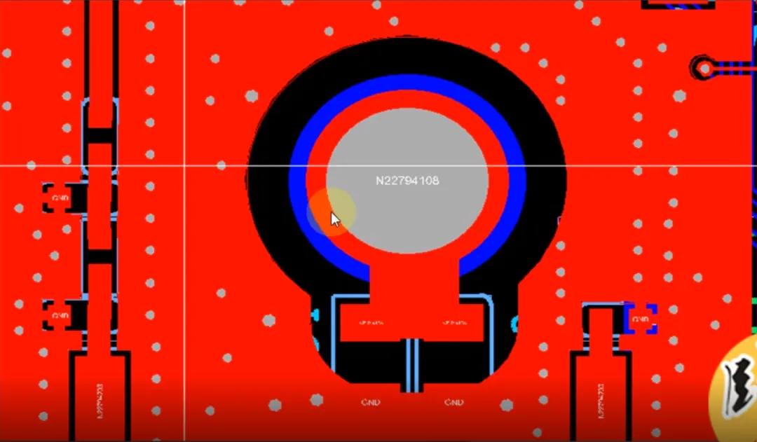
Figure 1 | Conceptual example of a parallel RC network tying PCB ground to chassis ground through a mounting point
What the Capacitor Does: AC Coupling to the Chassis
The capacitor provides an AC short between the PCB ground and the chassis at high frequency, while presenting a high impedance at low frequency and an open circuit at DC. Its reactance is Xc = 1/(2πfC). As frequency increases, the reactance falls, creating an effective return path for high-frequency common-mode currents and ESD energy to flow to the chassis instead of through sensitive circuits. This achieves a “block DC, pass AC” behavior at the board-to-chassis interface.
In practical terms, the capacitor helps:
- Shunt high-frequency interference and common-mode noise from the board to the chassis, reducing radiated and conducted emissions.
- Provide a low-impedance path for the high-frequency components of ESD events to reach the chassis, limiting the voltage rise of the PCB ground relative to the chassis during an ESD strike.
- Define the return path for high-frequency currents, improving signal integrity and reducing the loop area of common-mode currents that would otherwise couple to cables or enclosure seams.
The effective impedance at RF also depends on the capacitor's equivalent series resistance (ESR) and equivalent series inductance (ESL). Select capacitors with low ESL (e.g., multilayer ceramic capacitors, MLCCs) and place them with very short leads and wide connections to minimize parasitic inductance. At radio frequencies, parasitics dominate; a physically larger or poorly placed capacitor can lose effectiveness because its ESL raises the impedance right where you intended to reduce it.
Why Add a High-Value Resistor: DC Reference and Charge Bleed
A capacitor alone isolates DC between the PCB ground and the chassis. That means the board ground can float and accumulate charge relative to the chassis. Over time, or during handling, this charge can build to a level that causes latch-up, ESD damage, or nuisance behavior when the board finally discharges. The high-value resistor addresses this by providing a controlled DC path that gently equalizes potentials between the PCB ground and the chassis.
In the example values, a 1 MΩ resistor imposes negligible DC current under normal conditions while still offering a defined discharge path for static charge. The RC time constant is τ = R × C = 1 MΩ × 0.1 μF = 0.1 s. That time constant is long enough to avoid coupling hum and other low-frequency interference into the board, yet short enough to bring a floating ground toward the chassis potential over time. The resistor also limits current if an external static potential appears on the chassis, preventing a sudden surge through the PCB ground network that could stress ICs or reference nodes.
Important details when choosing the resistor include:
- Value: A high value, such as 1 MΩ, provides the desired “bleed” function with minimal DC coupling. Lower values increase the DC coupling and potential leakage current, while higher values may not discharge accumulated charge as effectively.
- Voltage and power rating: Select a resistor with appropriate voltage rating for the environments the product will face. Although steady power dissipation is trivial, the part must handle anticipated transient voltages without arcing or breakdown.
- Mechanical reliability: Use resistors with suitable construction for the environment (e.g., temperature cycling, vibration) to avoid cracking or drift.
Benefits for ESD and EMI Control
Many EMI and ESD problems stem from undefined or high-impedance return paths. The parallel RC tie clarifies the return path between the PCB ground and the chassis without creating a direct DC bond. In ESD scenarios, the fast-rising edge contains substantial high-frequency content. The capacitor offers a low-impedance path for that energy to the chassis, reducing the PCB ground's voltage excursion and lowering the risk of overstress to IC pins and interfaces. The resistor then bleeds any residual charge difference post-event.
From an EMI perspective, common-mode noise at the PCB ground is more effectively returned to the chassis when a high-frequency path exists. The capacitor provides that path and reduces the common-mode voltage that would otherwise drive antenna-like structures such as cables or seams. The result is often measurable improvement in both radiated and conducted emissions. Because DC and low-frequency coupling remains very weak, ground-loop currents that would introduce hum or offset errors in sensitive analog circuits are minimized.
Component Selection and Practical Considerations
While 0.1 μF and 1 MΩ are frequently seen, these values are not universal requirements. The optimal values depend on the system's frequency content, noise environment, and regulatory constraints:
- Capacitance: Larger values reduce impedance at lower frequencies but increase leakage at power frequencies through parasitics. Smaller values reduce leakage but may be less effective for lower RF frequencies. Choose a capacitance that balances EMI needs with allowable leakage and safety considerations.
- Capacitor type and rating: Use MLCCs with suitable voltage rating and low ESL. If the chassis is bonded to protective earth and mains safety is a concern, use capacitors with appropriate safety certifications for the application. Ensure adequate creepage and clearance around the chassis connection.
- Resistor value: Values in the high hundreds of kilohms to several megohms are common for a gentle bleed without meaningful DC coupling. Select based on how quickly you want the PCB ground to track the chassis potential and the acceptable leakage current in your application.
Remember that these values serve functional goals: the capacitor creates a low-impedance HF bond; the resistor sets the DC relationship and discharge time. Test and adjust as needed for your product's specific environment and compliance targets.
Layout and Mechanical Integration
Implementation quality can determine whether the RC connection works as intended. Follow these guidelines:
- Shortest possible path: Place the RC network close to the mechanical tie point to the chassis, such as a mounting hole or earth stud. Keep traces short and wide to reduce inductance.
- Solid connection to chassis: Use a dedicated pad or bonding point that ensures a reliable mechanical and electrical connection to the chassis. Metal standoffs or mounting hardware should provide a clean, low-impedance path.
- Single-point strategy: In many designs, a single, well-controlled board-to-chassis connection provides predictable behavior. Multiple connections can reduce impedance further at high frequency but may also create unintended loop paths at lower frequencies. Evaluate based on your noise environment and enclosure geometry.
- Minimize parasitics: Treat the RC path like an RF connection. Avoid vias and long narrow traces. If vias are unavoidable, use multiple vias in parallel to lower inductance.
- Shielding strategy: Combine the RC bond with good enclosure practices—continuity across panel seams, conductive gasketing where necessary, and controlled cable shield terminations—to form a coherent EMI control plan.
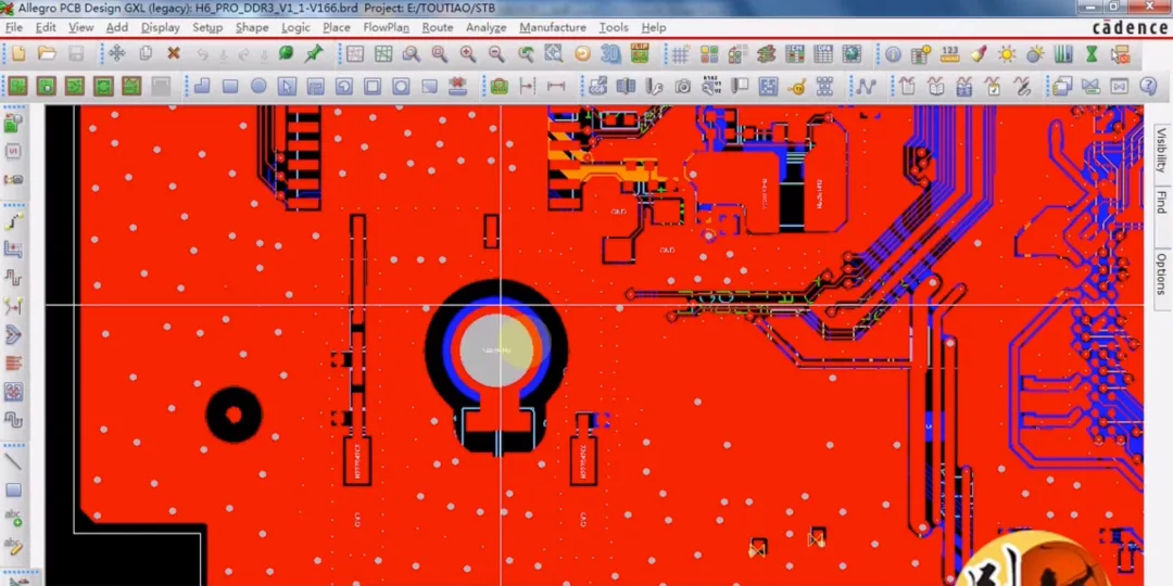
Figure 2 | Example placement of the parallel RC bond near a chassis mounting point
Common Pitfalls and How to Avoid Them
- Using only a resistor: A resistor alone presents high impedance at high frequency, which is ineffective for shunting RF noise or ESD to the chassis. The capacitor is essential for a low-impedance HF bond.
- Using only a capacitor: A capacitor alone blocks DC and low-frequency currents. Without the resistor, the PCB ground can float and accumulate charge, increasing the risk of ESD upset and unpredictable behavior.
- Poor placement: Locating the RC network far from the chassis contact point or routing through narrow, long traces adds inductance that undermines the HF bond.
- Underrated parts: Ensure both the capacitor and resistor have sufficient voltage and environmental ratings for the product's use cases, including ESD stress and transient exposure.
- Uncontrolled multiple bonds: Adding multiple RC bonds without considering loop formation can couple low-frequency interference into sensitive circuits. Plan the bonding scheme deliberately and validate with measurements.
Verification and Testing
Validate the effectiveness of the RC bond under realistic conditions:
- ESD testing: Apply contact and air discharges to enclosure points per your test plan and observe system behavior. Monitor ground potentials and verify that the PCB ground remains within safe limits relative to the chassis.
- EMI pre-compliance: Measure radiated and conducted emissions with and without the RC bond engaged (for example, by depopulating the components) to quantify its effect and refine values.
- Functional checks: Verify that sensitive analog or low-level measurements are not adversely affected by the bond. If necessary, adjust the resistor value to optimize the DC behavior without compromising EMI control.
Summary
Connecting PCB ground to the chassis through a parallel resistor and capacitor offers a pragmatic, effective way to manage both EMC and ESD challenges. The capacitor provides the essential high-frequency return path to the chassis, improving emission and immunity performance, while the high-value resistor establishes a controlled DC relationship and discharges accumulated charge. Thoughtful component selection, careful placement, and deliberate bonding strategy ensure the network performs as intended. Although 0.1 μF and 1 MΩ are commonly used, treat them as starting points rather than universal rules—measure, iterate, and select values that fit your design's specific noise environment and compliance requirements.