Electrostatic discharge (ESD) control is fundamental to reliable electronics manufacturing and test. Among the objects that require special attention are isolated conductors—conductive items that cannot be grounded or equipotentially bonded. In an ESD environment, these objects can accumulate charge and become a hidden source of discharge damage to ESD-sensitive devices. Isolated conductors are frequently encountered around semiconductor equipment, assembly and test workstations, and in any area where grounding is interrupted or impractical.
What Is an ESD Isolated Conductor?
Per ANSI/ESD S20.20, an isolated conductor is a conductor that cannot be directly grounded and cannot be equipotentially bonded to ground or to other conductors. Because it floats electrically, its potential may drift relative to grounded items and sensitive components, allowing significant surface charge to build. When the isolated item approaches or contacts a device lead frame, PCB pad, or exposed circuitry, a discharge can occur—often faster than a protection network can respond.
Key Characteristics of Isolated Conductors
- Insulation from ground: The conductor is insulated from ground, either directly or indirectly (e.g., mounted on plastic, painted, or anodized surfaces). This allows surface charge to accumulate.
- Lack of equipotential bonding: The conductor is not bonded to the same reference potential as surrounding conductive items or ground. Its voltage can differ substantially from other parts of the workstation, increasing the risk of discharge when contact occurs.
- Opportunity for contact: The conductor can come into contact with ESD-sensitive devices (ESDS). Examples include tools, fixtures, carriers, or machine parts that can touch devices or PCBs during assembly, test, and handling.
Where Do Isolated Conductors Appear in SMT and Test?
Common examples include:
- Metal hand tools stored on plastic trays or hung on painted racks.
- Machine parts, covers, or guards mounted on insulating bushings or painted/anodized structures.
- Test fixtures and nests with metallic inserts isolated by plastics or coatings.
- Feeder carts, reflow carriers, or conveyors with conductive sections interrupted by insulating joints.
- Robotic end-effectors and nozzles that are conductive but not bonded to the tool chassis ground.
These items often sit near or contact ESDS. Without a controlled path to ground, they can charge triboelectrically during handling or by induction from nearby fields, then discharge into devices.
Objective of Measurement
The primary objective is to quantify the surface potential (voltage) of isolated conductors and determine if they pose a hazard to ESDS under normal operating conditions. Measurement supports risk assessment, corrective actions (e.g., bonding, grounding, ionization), and periodic compliance verification.
Measurement Methods
Two instrument types are commonly used to measure the surface voltage of isolated conductors:
- Non-contact electrostatic voltmeters (also known as fieldmeters)
- Contacting electrostatic voltmeters with probes
Non-contact Electrostatic Voltmeter
Principle: A non-contact meter senses the electric field strength above a surface. With a known sensor-to-surface spacing, the instrument converts field strength to surface potential. The reading depends on distance and surface geometry, so proper standoff and instrument calibration are essential.
Advantages:
- No physical contact with the test object; little disturbance of the charge distribution.
- Fast and suitable for scanning larger areas.
Limitations:
- Accuracy degrades at low voltages (e.g., below about 35 V); resolution and noise may limit usefulness for very small potentials.
- Small, curved, or highly non-planar surfaces can yield less reliable readings due to geometry effects and fringing fields.
- Readings are highly dependent on probe distance and alignment; variation increases uncertainty.
Recommended procedure:
- Verify instrument zero and perform any required built-in calibration checks. Ensure the meter reference (chassis) is properly grounded according to the manufacturer's instructions.
- Set and maintain the specified sensor-to-surface distance using a spacer or integrated standoff indicator.
- Aim the probe normal to the surface (perpendicular) and hold it steady to minimize motion-induced errors.
- Measure at multiple points across the conductor, noting the distance setting and location for each reading.
- Record values with environmental conditions (temperature, humidity) and nearby sources of fields or airflow that could influence readings.
Contacting Electrostatic Voltmeter
Principle: A contacting probe touches the surface and senses charge at the point of contact. The instrument derives voltage using the relationship V = Q/C. High-input-impedance designs and appropriate probes are used to minimize charge transfer during measurement.
Advantages:
- High accuracy and repeatability, especially on small or irregular objects that challenge non-contact methods.
- Less sensitive to object geometry compared with non-contact meters.
Limitations:
- Physical contact can perturb the local charge distribution; measurements should be prompt and consistent.
- Probe contamination (oils, residues) can affect readings; cleanliness and probe selection matter.
Recommended procedure:
- Select an appropriate probe (metal or ceramic) per the object's surface and the instrument manufacturer's guidance. Clean the probe to remove contaminants.
- Ground the instrument per the user manual and zero it before use.
- Gently touch the probe to the isolated conductor at the designated point, ensuring stable, light contact.
- Read and record the voltage. Repeat at multiple locations to capture spatial variation.
- Document probe type, contact pressure approach (light touch), and any observed changes over repeated touches.
Tools and Equipment
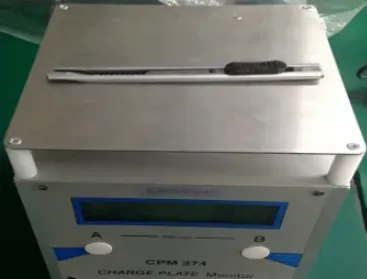
- Electrostatic voltmeter: Choose non-contact or contacting type based on object geometry, required accuracy, and expected voltage levels.
- Probes: For contacting meters, select the proper metal or ceramic probe and maintain it in a clean condition.
- Grounding equipment: Ensure the instrument, any reference surfaces, and the operator (e.g., via wrist strap) are grounded to the facility ESD ground as required.
- ESD personal and workstation controls: Gloves, ESD garments, and compliant work surfaces help reduce interference from operator charge and ambient fields during measurements.
Precautions and Good Practice
- Safety: Follow applicable safety procedures while working near powered equipment. Avoid creating discharge events during measurement that could affect devices or operators.
- Accuracy and interference: Confirm instrument zero and proper operation before measurements. Keep other electrostatic sources (ionizers, charged packaging, moving plastics) away from the measurement zone to avoid field coupling that biases readings.
- Environmental control: Manage temperature and humidity to reduce charge generation and improve measurement stability. Avoid direct airflow on the probe or object during readings.
- Documentation and analysis: Record voltage values along with object identification, measurement locations, instrument type, probe-to-surface distance (for non-contact), probe type (for contact), environmental conditions, and equipment calibration dates. Consistent documentation enables trend analysis and process control.
Interpreting Results and Next Steps
Measurement results should be evaluated in the context of the object's proximity to ESDS, the likelihood of contact, and process conditions. High absolute voltages indicate increased risk, but risk also depends on capacitance, discharge path, and device susceptibility. When risk is identified, consider the following mitigations:
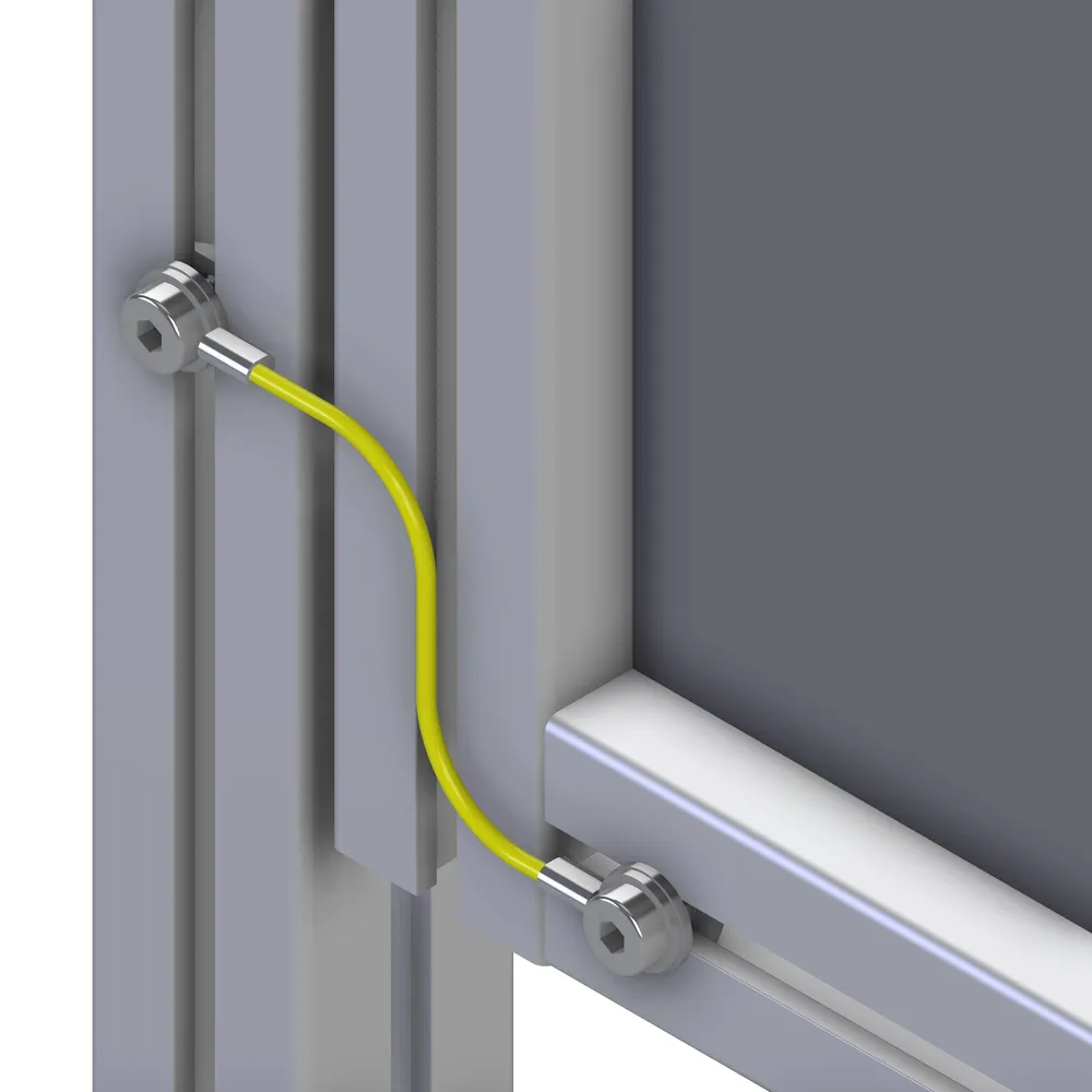
- Equipotential bonding/grounding: Where feasible, bond the conductor to ESD ground using appropriate hardware. Remove insulating coatings in the bond path to ensure a low-impedance connection.
- Provide a dissipative path: Replace purely insulating mountings with dissipative spacers or add bonding straps that allow controlled leakage to ground.
- Process and tooling changes: Modify handling to avoid incidental contact between isolated conductors and ESDS, or add covers and guards that prevent contact.
- Ionization: In areas where direct bonding is impractical, point-of-use ionization can help neutralize charge on isolated conductors and nearby insulators.
- Periodic verification: Recheck identified isolated conductors at defined intervals and after equipment maintenance or tooling changes.
Common Pitfalls and How to Avoid Them
- Unknown probe distance with non-contact meters: Always use a defined standoff. Small distance errors can cause large voltage errors.
- Attempting non-contact readings on very small or curved features: Switch to a contacting voltmeter when geometry prevents reliable field-to-voltage conversion.
- Contaminated contact probes: Clean probes regularly. Residues can create leakage paths or unstable contact, skewing results.
- Measuring transient conditions without stability: Allow the environment to stabilize (e.g., stop nearby material handling or airflow) before recording values.
- Neglecting operator charge: Ensure the operator is grounded and wearing appropriate ESD apparel to avoid coupling charge into the measurement.
Conclusion
Isolated conductors are a critical focus of any ESD control program. Because they cannot be directly grounded or equipotentially bonded, they can accumulate charge and present a discharge threat to sensitive devices in SMT assembly and test. By selecting the appropriate measurement method—non-contact for rapid, non-intrusive scans or contact measurement for accuracy on small or irregular items—engineers can quantify surface potential and assess risk with confidence. Accurate measurement depends on proper grounding, instrument setup, control of environmental influences, and thorough documentation.
When elevated voltages are discovered, practical countermeasures include equipotential bonding, adding dissipative paths, adjusting tooling and handling to eliminate contact risk, and applying ionization where bonding is impractical. Regular verification and maintenance keep ESD risks under control, enabling stable, high-yield electronics manufacturing.