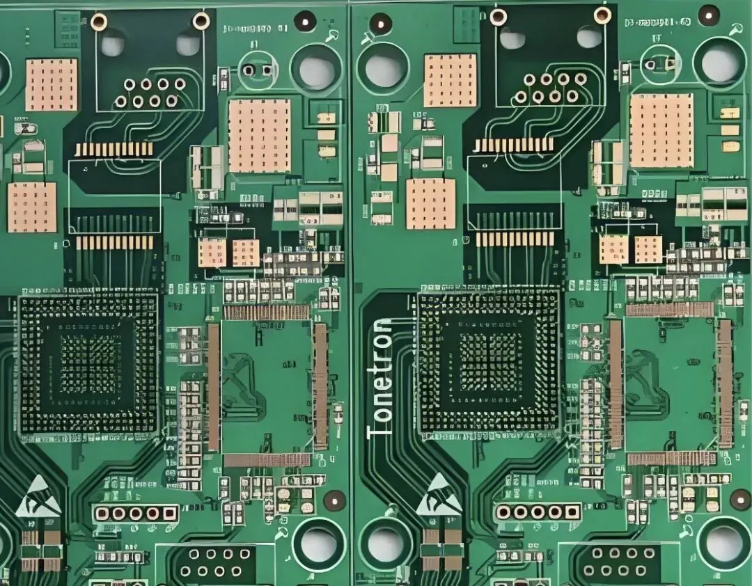
Placing BGA components on both sides of a PCB is a common way to increase component density and make better use of limited board area. However, this approach introduces significant challenges in both PCB fabrication and SMT assembly. The main concerns involve thermal stress, board warpage, routing density, power integrity, solder-joint reliability, reflow-process control, inspection, and rework.
Fabrication Challenges
The fabrication-related challenges primarily occur during PCB manufacturing and affect the board's mechanical and electrical performance.
Thermal Stress and Board Warpage
A PCB with BGA components on both sides may pass through multiple high-temperature reflow operations. Repeated heating can increase expansion along the board's Z-axis. If the laminate has an insufficient glass-transition temperature, or Tg, the PCB may experience excessive deformation during heating and cooling.
When BGAs are installed on both sides, the distribution of thermal and mechanical stress becomes more complicated. Uneven copper density, different component masses, and the locations of large copper planes can all contribute to nonuniform deformation. Board warpage is particularly critical for BGA packages because the solder joints are distributed across a relatively large area. Corner solder joints may experience additional mechanical stress when the package and PCB do not remain coplanar, increasing the risk of cracking.
Warpage can also reduce the contact quality between the PCB pads, solder paste, and BGA balls during assembly. Even if the center of the package remains relatively stable, lifted corners or a distorted board surface may produce open joints, uneven collapse, or inconsistent solder-joint geometry.
High Routing Density and Complex Stackup Requirements
Fanout routing for BGAs on both sides requires a large number of vias. If the two BGA patterns overlap in their vertical projection, conventional through-vias may interfere with one another or create unwanted electrical connections between layers. In such cases, a standard through-hole structure may not provide enough routing flexibility.
Blind vias, buried vias, or an any-layer HDI structure may then be required. These technologies can provide additional routing channels around and beneath the BGA escape region, but they also increase fabrication complexity and cost. The stackup must be planned before placement and routing begin. The designer needs to determine which regions can use through-vias and which regions require blind or buried structures.

The routing problem is not limited to signal escape. Via placement also affects reference-plane continuity, power distribution, thermal conduction, and manufacturability. A dense fanout region can consume the routing space needed for power and ground connections, making early stackup planning essential.
Power Integrity Constraints
The area directly beneath or behind a high-performance BGA is often an ideal location for decoupling capacitors. Keeping the capacitor close to the device reduces the current-loop area and helps lower the effective impedance of the power distribution network.
When another BGA occupies the opposite side of the same region, there may be insufficient room for the required capacitors, vias, or power connections. The increased distance and restricted routing path can raise power-distribution impedance and reduce the effectiveness of high-frequency decoupling. For devices with fast transient current demand, this may affect operating stability even when the DC power voltage appears correct.
Power and ground planes must therefore be considered together with BGA placement. The designer should reserve space for decoupling components and their connections before finalizing the location of the second-side BGA.
SMT Assembly Challenges
Assembly-related challenges occur mainly during solder paste printing, component placement, reflow, inspection, and repair. They directly affect production yield and long-term reliability.
Reliability Problems Caused by the Second Reflow
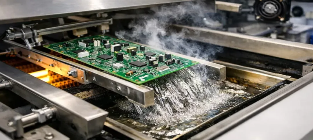
When the second side of the PCB is assembled, the BGA solder joints on the first side may pass through another complete reflow cycle. This second reflow exposes the previously formed joints to additional heating and cooling, which can alter their microstructure and mechanical condition.
Repeated thermal exposure may increase the thickness of intermetallic compounds, or IMCs, within the solder joint. Although an intermetallic layer is necessary for metallurgical bonding, excessive growth can make the joint more brittle. Under mechanical or thermal stress, the joint may then be more susceptible to cracking.
Liquid solder during reflow may also experience dewetting. If the solder does not maintain a stable bond with the pad or the IMC interface, cracking or local separation can occur at the interface. These defects may be hidden beneath the BGA package and remain undetected without suitable inspection.
Component Drop and Position Shift
During second-side reflow, the solder joints formed on the first side may melt again. If a first-side BGA is relatively heavy, the molten solder may not provide enough mechanical support to hold the package in position. Gravity can cause the component to drop, tilt, or shift.
The risk depends on package mass, solder-joint condition, board orientation, and the reflow process. A shifted BGA may produce misaligned joints, bridging, opens, or uneven solder collapse. For this reason, the assembly sequence should account for component size and mass rather than treating both sides as equivalent.
BGA Shadowing and Conflicting Thermal Requirements
When BGAs are installed on both sides, a large BGA on the second side can obstruct hot-air flow or infrared radiation. Smaller components and solder joints located around or beneath the package may then receive less heat than expected.
The two sides of the PCB may also have different thermal capacities because of differences in package size, copper distribution, component density, and exposed board area. A single reflow profile may not heat both sides uniformly. If the profile is optimized for one side, the other side may experience insufficient heating, excessive temperature exposure, voiding, or cold solder joints.
Thermal profiling should therefore consider the actual component arrangement rather than relying only on a nominal oven setting. The objective is to reduce the temperature difference across the board while still meeting the melting and process requirements of the solder system.
Inspection and Rework Difficulties
BGA solder joints are hidden beneath the package body, so visual inspection cannot verify the complete joint array. X-ray inspection is normally required to identify opens, bridges, voids, misalignment, and other hidden defects.
When BGAs on opposite sides overlap in projection, the X-ray images may interfere with one another. Overlapping packages, solder joints, and vias can make image interpretation more difficult and reduce inspection efficiency. This is another reason to avoid unnecessary vertical overlap during placement.
Rework is even more challenging. Local heating applied to one BGA can transfer heat through the PCB and remelt the solder joints of the BGA on the opposite side. The opposite component may then shift or fall from the board. Rework equipment must therefore control the heating area carefully and use thermal shielding or mechanical support to protect the other side.
Design and Manufacturing Optimization
Placement and Layout Strategy
Wherever possible, avoid placing two BGAs directly opposite each other. Reducing vertical overlap simplifies via planning, improves X-ray interpretation, provides more room for decoupling capacitors, and helps distribute thermal and mechanical stress.
If overlap is unavoidable, the design may require blind or buried vias and an HDI stackup. A large BGA can be placed on one side and a smaller BGA on the other, with the two packages offset as much as practical. Staggering their positions helps prevent concentrated stress and reduces interference between fanout structures.
Material Selection
A laminate with a high Tg, such as a material with Tg above 170 °C, can help reduce deformation during repeated high-temperature processing. Low-moisture-absorption materials are also preferable because absorbed moisture can contribute to dimensional changes and reliability problems during heating.
Material selection should be coordinated with the expected reflow sequence, board thickness, copper distribution, and component density. The laminate alone cannot eliminate warpage, but an appropriate material provides a more stable foundation for the complete design.
Stackup, Power, and Thermal Design
Define the stackup early and assign through-vias, blind vias, and buried vias according to the available routing space. Non-overlapping regions may use conventional through-vias, while overlapping BGA areas may require higher-density interconnect structures.
High-power BGAs should also include an appropriate thermal-via arrangement to transfer heat into the relevant copper planes. Heat sources should be distributed where possible instead of being concentrated directly opposite one another. At the same time, sufficient space must be reserved for power and ground connections, decoupling capacitors, and short current-return paths.
Assembly Sequence and Process Control
The assembly sequence should consider package size and mass. A smaller or heavier BGA may be assembled on the bottom side first, followed by the larger BGA on the top side, reducing the likelihood of component drop during the second reflow. Depending on the design and process capability, adhesive or underfill may also be used to reinforce a BGA that has already been assembled.
The second reflow should have its own optimized thermal profile. The process should minimize the temperature difference across the board and avoid excessive thermal exposure to the first-side solder joints. Where process conditions permit, nitrogen reflow can help reduce oxidation and may improve control of soldering defects and voiding.
Dedicated fixtures can support and protect first-side components while the second side is assembled. During rework, localized heating and thermal shielding should be used to prevent the opposite-side BGA from reaching a temperature at which its solder joints melt.
Conclusion
Placing BGAs on both sides of a PCB is an effective space-saving strategy, but it transfers additional complexity into fabrication and assembly. Success depends on coordinated decisions made early in the design process, including laminate selection, stackup planning, BGA placement, via structures, decoupling access, and thermal management. Manufacturing and SMT teams must then control the assembly sequence, reflow profile, support tooling, X-ray inspection, and rework method. The closer these activities are coordinated, the lower the risk of warpage, hidden solder-joint defects, component displacement, and power-integrity problems.