










A low dropout regulator (LDO) is a linear voltage regulator that provides a regulated output with a small dropout voltage between input and output. It is commonly used to step down a higher DC voltage to a stable lower voltage for sensitive loads. At a high level, an LDO integrates a reference, an error amplifier, and a pass device to maintain a fixed voltage difference between its output and the reference, regulating the output even as input voltage and load current vary.
LDOs are widely used in mobile devices, communications equipment, embedded systems, and any application that requires a clean, low-noise supply for analog or digital circuits. They are especially attractive when the input-to-output voltage difference is small, the load current is moderate, and noise performance is important.
Key Characteristics of LDO Regulators
- Low dropout voltage. The dropout voltage of an LDO typically ranges from several hundred millivolts to a few volts, enabling regulation even when the input is only slightly above the desired output. This makes LDOs useful for post-regulating a switching supply or deriving lower rails from a higher battery voltage.
- Stable output regulation. LDOs provide a stable, regulated output over a range of input voltages and load currents. They often exhibit good power-supply rejection ratio (PSRR) and inherent noise attenuation thanks to their linear architecture and feedback control.
- Low quiescent power and low noise. Because LDOs are linear devices and do not switch, they can achieve low quiescent current and low noise. Overall efficiency, however, depends on the voltage drop and load current. The power dissipated as heat equals (Vin ? Vout) × Iout, which must be handled by the PCB and package thermal design.
- Fast transient response. Many LDOs offer relatively fast response to load changes due to their internal control loop design. Proper selection and placement of input and output capacitors are critical to achieving the specified transient and stability performance in a real PCB.
In practice, realizing the datasheet performance of an LDO depends heavily on PCB layout quality. The placement of the regulator relative to its input source, the output load, and the associated decoupling components has a direct impact on regulation accuracy, noise, transient response, and thermal behavior.
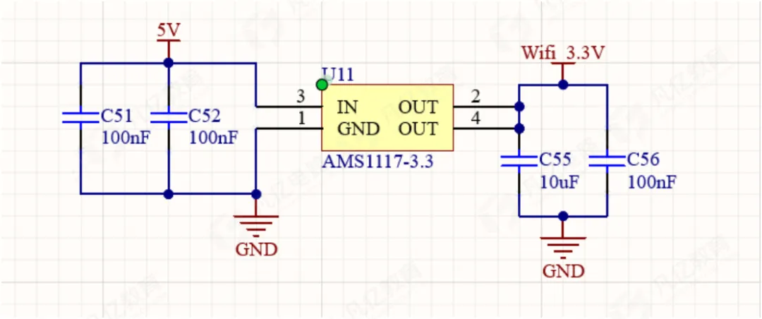
LDO PCB Layout Guidelines
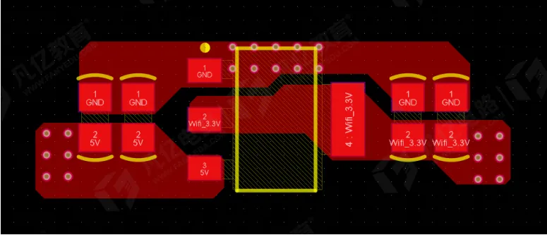
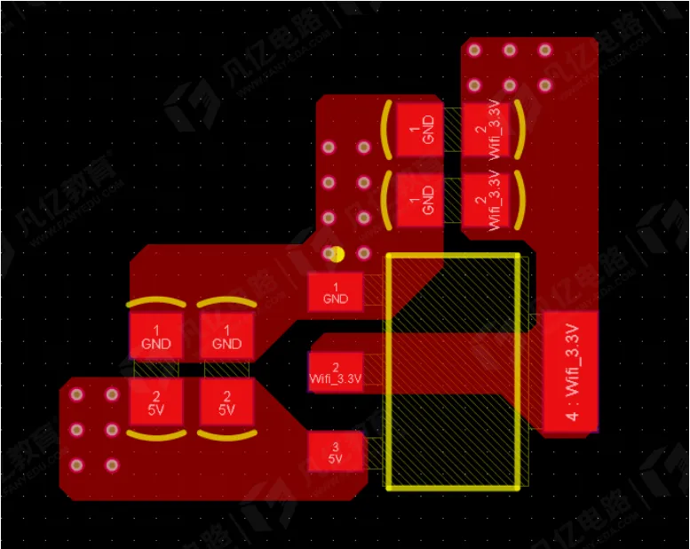
Effective LDO layout is fundamentally about controlling current paths, minimizing loop area, and ensuring the LDO sees the capacitors and the load as intended by the datasheet. Two placement strategies are commonly used: a straight-line topology or an L-shaped topology. In both cases, the objective is to keep the current loop small and the connections short and direct.
- Analyze input and output paths; use straight-line or L-shaped placement with the smallest possible loop. Arrange the input bulk capacitor, input bypass capacitor, LDO, and output capacitors so that the high-current path runs in a compact, contiguous loop. In a straight-line layout, the sequence typically follows Input Source → Input Capacitors → LDO → Output Capacitors → Load. In an L-shaped layout, maintain the same sequence while turning the path to suit board constraints. The priority is to minimize the physical distance between each element in the power path and to keep the loop area small to reduce parasitic inductance and radiated/received noise.
- Place input and output capacitors in the order of large to small. Provide a larger bulk capacitor (for example, an electrolytic or larger MLCC) to handle low-frequency load variations and supply impedance, and a small, low-ESR ceramic capacitor very close to the pins to handle high-frequency transients and ensure loop stability. Place the small MLCC closest to each LDO pin (input and output respectively), with the bulk capacitor immediately behind it. This ordering ensures that the LDO “sees” a low-impedance source and load at high frequencies while still having sufficient bulk energy nearby.
When laying out capacitors, observe the datasheet’s minimum and recommended capacitance and ESR ranges. Many LDOs require a certain output capacitor ESR or a minimum capacitance for stability. Excessively high series inductance from long traces or distant capacitors can undermine stability and transient response.
LDO PCB Routing Guidelines
Routing for an LDO must support both DC current capacity and AC performance. The goals are to minimize IR drop in the supply path, provide robust return current paths, and prevent noise from coupling into sensitive nodes.
- Ensure power traces and via count meet current-carrying needs. Size the input and output traces for the expected load current and allowable voltage drop. Use multiple vias in parallel for transitions to other layers to reduce via resistance and inductance. Wider copper reduces DC losses and helps distribute heat.
- Place the input via before the first input capacitor; place the output via after the last output capacitor. If the input or output must transition layers, bring the input onto the LDO plane before the first input decoupling capacitor so the capacitor directly shunts the source impedance. Likewise, route the output from the LDO through the output capacitors first, with any layer transition or remote routing occurring after the final output capacitor. This preserves the intended decoupling order and ensures the LDO experiences a low-impedance environment at its pins.
- Make the GND return path robust; place ground vias near the LDO ground pin. Provide a wide, low-impedance ground path for input and output capacitor returns. Place ground vias close to the LDO ground pad or ground pin so that return currents close through the smallest possible loop. Avoid forcing high-current returns to detour across the board.
- Connect input and output grounds together to ensure a solid return path. Tie the input and output ground networks at or near the LDO ground node to provide a contiguous return path. This star-like connection at the LDO ground reduces the risk of noise coupling from the input side into the output, and ensures that the LDO loop is closed locally. Avoid separating grounds in a way that extends the return current path or creates ground potential differences around the regulator.
Component Selection and Placement Considerations
Beyond the basic placement and routing rules, a few component-level considerations are crucial to achieving stable and low-noise performance:
- Input capacitors. Choose a combination of bulk and ceramic capacitors to manage both low-frequency and high-frequency impedance. Place the ceramic capacitor as close as physically possible to the LDO input pin and ground, with short, wide traces. The bulk capacitor should be close behind it. For long input feeds or high di/dt loads, additional bulk reservoir capacitance near the LDO mitigates line dips.
- Output capacitor ESR and stability. LDO stability often depends on the output capacitor’s ESR and value. Many modern devices are stable with low-ESR MLCCs, while others need some ESR. Follow the datasheet recommendations and avoid long traces that add unwanted series inductance. Place the output ceramic capacitor adjacent to the output pin and ground.
- Sensitive nodes. If the LDO has an ADJ/FB pin (for adjustable versions), keep the feedback divider compact and close to the LDO, route the feedback node away from noisy nets, and connect the bottom of the divider to the LDO ground at the same point as the output capacitor return to avoid ground errors. Do not run the feedback trace next to high-current paths.
- Load placement. When possible, place the primary load near the LDO output to reduce IR drop and loop inductance. For remote loads, consider a sense line (if supported) or account for voltage drop by adjusting the setpoint.
Grounding and Return Current Control
Good grounding is essential for LDO performance. The small-signal error amplifier inside the LDO compares the output (or a divided version) against its reference. Any noise injected into the ground reference or the feedback path directly affects regulation. To control return currents:
- Keep the input and output capacitor grounds close and connected at the LDO ground node. This confines high-frequency return currents to a tight local loop.
- Provide a solid ground plane underneath the LDO and its capacitors when possible. A continuous ground plane lowers loop inductance and provides a defined return path.
- Avoid splitting the ground plane under the LDO loop. If ground segmentation is required elsewhere, maintain an unbroken ground region for the LDO and its decoupling network.
Thermal Management on the PCB
Although LDOs are simple and low-noise, they dissipate power equal to (Vin ? Vout) × Iout. Depending on the load and voltage drop, this can result in significant heat that must be managed. PCB practices that improve thermal performance include:
- Use copper area as a heat spreader. Connect the LDO package’s thermal pad (if present) to a ground plane or a dedicated copper area. Larger copper pours reduce thermal resistance from junction to ambient.
- Add thermal vias. Place an array of vias under the exposed pad to conduct heat into inner or opposite-side copper planes. Ensure the vias are plated and connect to copper areas that can dissipate heat.
- Balance electrical and thermal needs. While widening copper for heat is beneficial, do not compromise the short, direct routing of input/output capacitors and ground returns. Integrate thermal and electrical objectives in the PCB layout.
Noise, PSRR, and EMI Considerations
LDOs provide intrinsic noise filtering and PSRR, particularly at lower frequencies. However, PSRR degrades at higher frequencies, and poor layout can allow input ripple or digital noise to couple into the output. To maximize noise performance:
- Keep the input decoupling loop small so that high-frequency noise on the input is locally shunted to ground before it reaches the LDO pin.
- Keep the output decoupling loop compact to provide a low-impedance path for load transients and to stabilize the control loop.
- Isolate sensitive analog loads from noisy digital domains by careful routing and ground return planning. If necessary and supported by the system design, additional filtering at the LDO input can reduce conducted noise into the regulator.
Common Pitfalls and How to Avoid Them
- Capacitors too far from the LDO pins. Long traces add inductance that defeats decoupling effectiveness and can destabilize the LDO. Place small MLCCs adjacent to the input and output pins.
- Layer transitions in the wrong place. Placing a via between the source and the input capacitor, or between the LDO and the output capacitor, inserts unwanted impedance. Ensure input vias precede the first input capacitor and output vias follow the last output capacitor.
- Inadequate ground return width. A narrow ground return increases impedance and noise susceptibility. Use wide ground traces or planes, and place ground vias near the LDO ground pin.
- Ignoring thermal dissipation. Failing to provide copper area and thermal vias can cause overheating under load. Estimate power dissipation and design copper accordingly.
- Overlooking feedback integrity. For adjustable LDOs, a poorly routed feedback path can cause output error or oscillation. Keep the divider close and reference it to the correct ground node.
By following these placement, routing, grounding, and thermal practices, an LDO can deliver the low-noise, stable voltage that many systems require. The simplest way to validate a layout is to verify the transient response and output stability with the intended load profile, and to ensure that the input and output decoupling capacitors are both electrically and physically as close to the LDO as the datasheet recommends.






