Many microcontroller pins are multiplexed: the same physical pad can serve as a general-purpose I/O (GPIO) or as a peripheral signal such as I2C, SPI, UART, PWM, or ADC. In schematic capture, clearly communicating which function a pin will use is essential for both readability and correct netlisting. KiCad's Alternate Pin feature lets you switch the functional label for a given pin on the schematic without changing its physical pin number, making it straightforward to represent multiplexed pins accurately and to keep your schematic consistent with firmware configuration.
What Are Alternate Functions on MCU Pins?
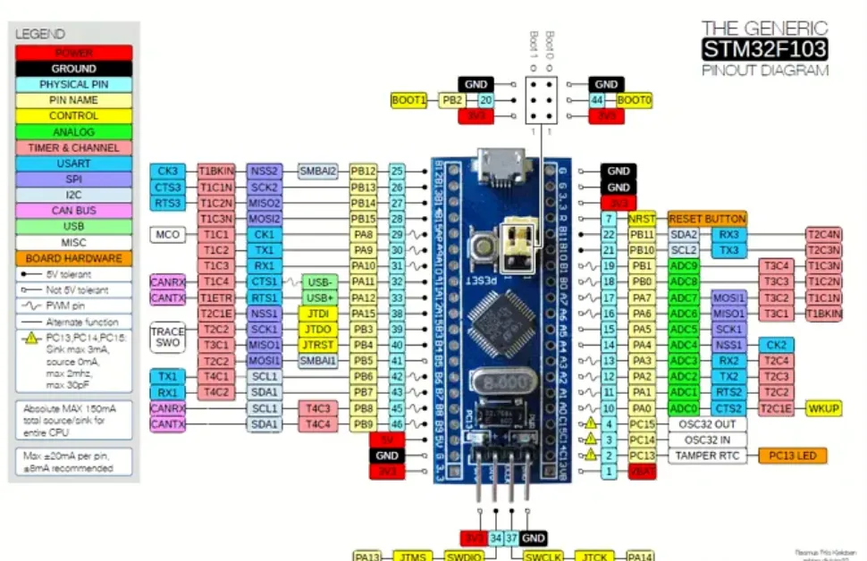
On most microcontrollers, the "normal" pin function refers to GPIO. As GPIO, a pin can be read or driven directly through standard I/O registers. The "alternate" functions are additional roles assigned to that same pad through a pin multiplexer, such as I2C SCL/SDA, SPI MISO/MOSI/SCK/CS, USART TX/RX, CCP/PWM outputs, timer channels, clock outputs, or analog inputs for an ADC. When a pin is configured for an alternate function, control is typically handed over to the corresponding peripheral via special function registers; the peripheral hardware then drives timing and behavior.
For example, in the STM32F103 series, pins PA0 through PA3 can each serve multiple alternate functions in addition to their primary I/O role. The device datasheet lists the available options per pin and how they are selected. This variety allows designers to route peripheral signals flexibly, but it also means the chosen function must be explicitly captured and communicated in the schematic to avoid ambiguity.
The default function after reset depends on the device; it is not always GPIO. Always check the datasheet to confirm the reset state. In most cases, firmware can select the desired function at runtime, switching between peripheral roles as needed. However, because a single pad cannot drive multiple roles simultaneously, designs must be structured so each multiplexed pin has a single active function at any given time. This constraint influences both hardware pinout planning and firmware pin-mux configuration.
Multiplexing allows one package to support a wide range of peripheral combinations, but there is a trade-off: while the microcontroller is capable of many functions, a given design usually assigns each pad a specific role that remains consistent throughout operation. Capturing that choice clearly in the schematic is critical for downstream PCB layout, netlist generation, and firmware coordination.
Using Alternate Pins in KiCad
When drawing a microcontroller symbol, there are two simple, yet imperfect, approaches often seen:
-
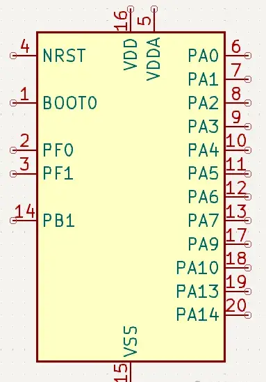
Only label each pin with its primary function. The symbol remains clean and readable, but the alternate roles are lost. Engineers must rely on external notes or datasheets to know which peripherals are possible, and confusion or miswiring can result.
-
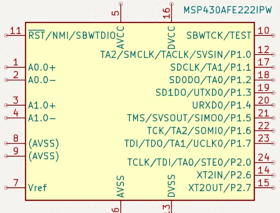
Concatenate all possible functions into the pin name separated by slashes. While this documents the options, the labels become long and cluttered, making the symbol harder to read. You may still need annotations to indicate which function is actually being used in the design.
KiCad's Alternate Pin feature solves these issues elegantly. Each pin retains a single physical pad number, while you can provide multiple functional labels. On the schematic, you select which functional label to display and to use in the netlist for that specific design instance. This keeps symbols tidy, improves readability, and ensures the netlist reflects the actual intended signal names.
Defining Alternate Pins in the Symbol Editor
To define alternate functions for a pin while creating or editing a symbol:
- Open the Symbol Editor and double-click the pin to open the Pin Properties dialog.
- Enter the primary function in the Pin name field. This is typically the GPIO name or the function you expect to use most often.
- In the Alternate pin definitions table, add additional functional names for the same pin number. You can add as many alternates as necessary to cover the device's pin-mux options.
By capturing alternates in the library, every schematic where the symbol is used gains the same clarity and flexibility. The physical pin number remains constant, so PCB footprint mapping is preserved regardless of which functional label is selected in a particular design.
Selecting Pin Functions in the Schematic
After placing the symbol onto a schematic sheet, you can choose which function each multiplexed pin uses in that specific design:
- Double-click the symbol to open the Symbol Properties dialog.
- Switch to the Pin functions page. For each pin with alternates, select the desired function from the list.
Confirm your selections and return to the schematic. The displayed pin names update automatically to reflect the selected functions, so the schematic clearly indicates which peripheral signals are assigned.
This approach documents all available options while keeping the schematic focused on the configuration actually used. It also reduces the need for ad-hoc notes and helps prevent wiring mistakes when multiple possible signals could occupy the same pad.
Practical Notes and Tips
Default function selection. When authoring library symbols, choose a sensible primary function to display by default, such as the GPIO name or the function most common in your organization's designs. This helps schematic readers quickly recognize the expected role without immediately diving into alternate choices.
Align firmware and schematic. The alternate pin label you choose in the schematic should match the intended firmware pin-mux configuration. Consistency ensures that the schematic net names correspond to the firmware's peripheral assignments, making cross-referencing easier during bring-up and debugging.
Plan for mutually exclusive roles. A single pad cannot drive two alternate functions simultaneously. When assigning peripherals across multiplexed pins, consider resource conflicts upfront. The schematic should show only one selected function per pin to convey the true connectivity and to avoid misleading parallel connections.
Net naming and netlists. Using alternate pin selections yields meaningful net names in the netlist without needing long, slash-separated labels. Clear net naming aids ERC checks, improves cross-probing in the EDA tool, and helps the layout engineer understand signal intent directly from the schematic.
Documentation and reviews. Capturing alternate functions in the symbol library centralizes device knowledge. During design reviews, reviewers can quickly see what other roles a pin could take if a re-spin or variant requires changes, all without cluttering the baseline schematic.
KiCad version support. Alternate Pins are supported starting in KiCad 7 and further refined in KiCad 8. Combined with the Pin Helper introduced in KiCad 8, you can more quickly generate standard net labels for common peripherals, leading to cleaner netlists and more consistent naming conventions across projects.
Library maintenance. When adding alternates, follow consistent naming conventions for functions (for example, use standard peripheral abbreviations like SPI_SCK, I2C_SDA, USART_TX). Consistency makes it easier to search, filter, and script across libraries and projects. If your team uses custom templates or symbol libraries, document the naming scheme so all designers apply alternates uniformly.
Verification against datasheets. Before finalizing a symbol's alternate functions, cross-check the list with the latest device datasheet to ensure accuracy. Pin-mux options can vary by package, device variant, or silicon revision. Keeping library definitions accurate prevents mislabeling and downstream rework.
Schematic hierarchy and reuse. Alternate Pins are especially helpful in hierarchical designs or reusable blocks. A symbol can remain generic while each project-specific instance selects the alternates appropriate for that design. This reduces the need to maintain multiple symbol variants for the same device.
Communication with layout and test. Clear alternate function selection aids handoff to PCB layout by ensuring net names reflect the actual peripheral roles. It also helps test engineers prepare appropriate test points and procedures, especially for interfaces like UART, I2C, or SPI that might otherwise not be obvious from generic GPIO labels.
Conclusion
Multiplexed pins are ubiquitous in modern MCUs and SoCs. The Alternate Pin capability in KiCad provides a practical way to document and select those functions directly within the schematic, keeping symbols clear, netlists accurate, and designs aligned with firmware configuration. With support introduced in KiCad 7 and improvements in KiCad 8—alongside tools like the Pin Helper—designers can capture complex pin-mux options without sacrificing readability or consistency.
Adopting this workflow not only streamlines schematic capture but also reduces integration errors and accelerates collaboration across hardware, firmware, and test engineering. Define alternates once in the library, select them per-instance in the schematic, and let KiCad propagate the correct functional names throughout your design artifacts.