 00:42
00:42
Pad Spacing
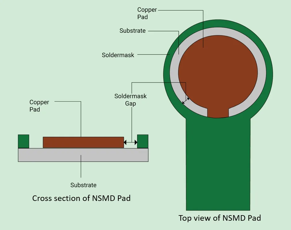
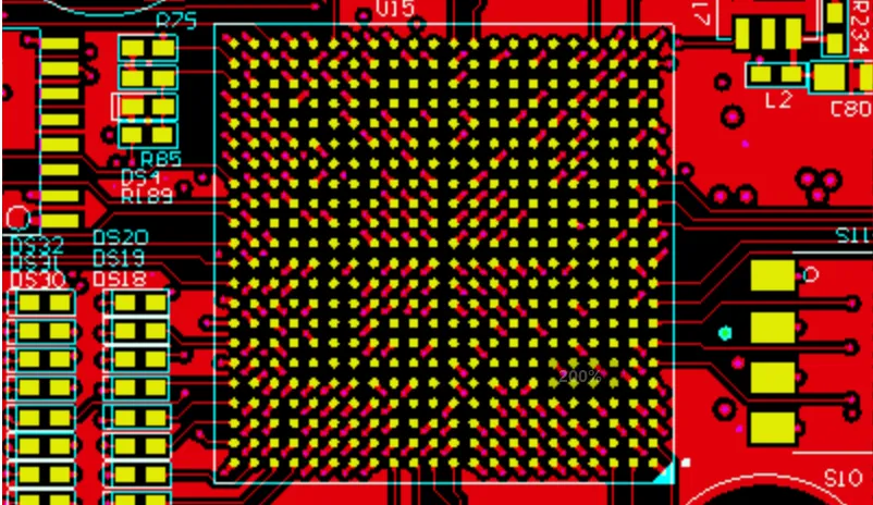
Pad spacing is a critical aspect of printed circuit board (PCB) design that determines the distance between conductive pads, directly impacting the board's reliability, manufacturability, and electrical performance. In electronics engineering, proper pad spacing helps prevent issues such as solder bridging, electrical shorts, and signal interference, especially in high-density layouts where components are closely packed. For designers and hobbyists searching for information on pad spacing, this tag aggregates articles that delve into the fundamentals, offering clear explanations of how spacing affects assembly processes like wave soldering or reflow techniques. Understanding these principles ensures compliance with industry standards such as IPC-7351, which provide guidelines for minimum clearances based on factors like voltage levels, board material, and environmental conditions. Practical applications of pad spacing extend to various scenarios, from consumer electronics to industrial automation. For instance, in surface-mount technology (SMT), maintaining optimal spacing around fine-pitch components like QFN packages can significantly reduce defect rates during production. Best practices include incorporating design rule checks (DRC) in CAD software to verify spacing early in the design phase, as well as considering thermal expansion and creepage distances for high-voltage applications. Engineers often adjust pad spacing to accommodate automated assembly lines, balancing compactness with ease of inspection and repair. By applying these insights, you can enhance PCB longevity and minimize costly revisions. The resources under this pad spacing tag include detailed tutorials on calculating ideal distances, case studies from real-world projects, and tips for troubleshooting common spacing-related errors. Reviewing these articles can provide the actionable knowledge needed to refine your designs, whether you are optimizing a prototype or scaling up for mass production.
Video Guide
-
00:42
Technical Articles
Get in Touch
Send Message
- Products & Service
- Company
- About AIVON
- Contact
- News
- Blog
- Certification
-


- Payment
-


2026 AIVON.COM All Rights Reserved