6-layer boards with 4mil line/space, 2oz outer copper, and mixed via treatments frequently require careful DFM review. This engineering case covers a real 6-layer FR-4 design that triggered several important engineering questions during CAM analysis. As a senior CAM engineer with over 15 years of experience, I regularly encounter mismatches between fabrication notes and actual design data that can impact assembly reliability and yield.
This project involved impedance control, resin-plugged vias, and dense IC areas. The article details the key issues we identified, the manufacturing risks, and how we resolved them through customer confirmation.
Order Overview
This was a 6-layer FR-4 PCB( #FR4-20260403-018 ) using TG150 material with a finished thickness of 2.0mm. Copper weights were 1oz inner layers and 2oz outer layers. Minimum hole size was 0.2mm with 4mil line/space. Surface finish was ENIG with red solder mask and white silkscreen. The design included impedance control with report and 100% flying probe testing. Certain vias required resin plugging. Panelization was 1x1 with mechanical forming. Quantity was 20 pieces (20 sets).
While the overall parameters were typical for a mid-range multilayer board, the combination of mixed via mask treatments, tight features in IC areas, and conflicting documentation created multiple production risks that needed clarification before fabrication.
Main Engineering Questions Found During CAM Review
Inconsistent Via Solder Mask Treatment
Some vias had solder mask openings while others were covered. This inconsistency was noted across multiple layers. We also identified large openings that potentially required resin plugging.
Figure 1: some vias had solder mask openings while others were covered
Our engineer asked for specific confirmation because mixed via mask treatments can lead to unpredictable solder behavior during assembly. We noticed this during solder mask data analysis. If ignored, open vias in dense areas could allow solder wicking, causing shorts or voids, while covered vias might trap air or flux residue. According to IPC-A-600 acceptability criteria, inconsistent via protection increases assembly defect risk.
The customer clarified the intended treatment, helping us avoid potential reliability issues in the final product.
Tight IC Pad Spacing and Solder Mask Bridge Limitation
After compensation for the 2oz outer copper, the spacing between IC pads in some areas was reduced to only 0.09mm. This was too tight for our standard solder mask process to guarantee reliable bridges.
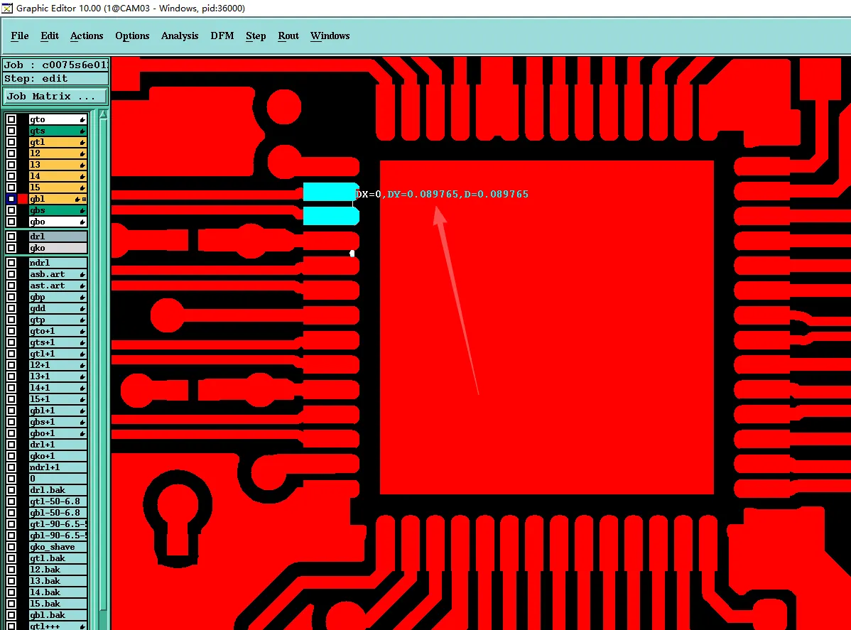
Figure 2: the spacing between IC pads in some areas was reduced to only 0.09mm
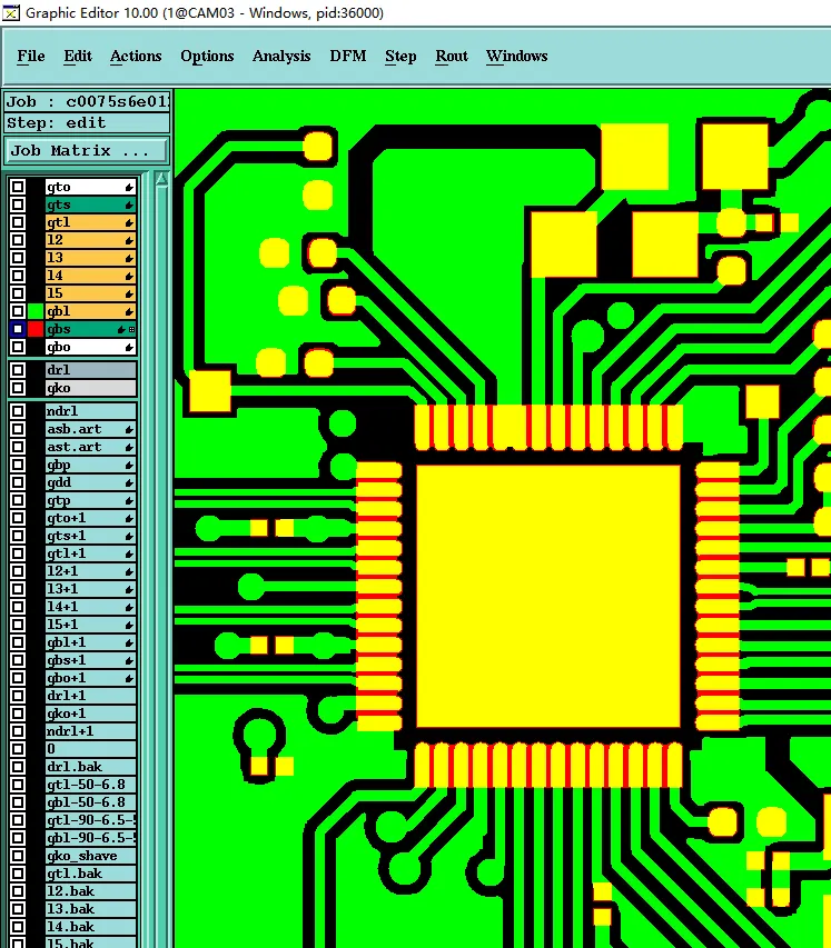
Figure 3: tight IC pad spacing
We noticed this during the solder mask review and raised the issue because fine-pitch IC areas are highly sensitive to mask performance. If production had continued without confirmation, the lack of solder mask bridges could result in solder bridging during SMT assembly, leading to short circuits, poor yield, and potential board scrap. We confirmed acceptance of no-bridge conditions in these critical areas.
NPTH Holes with Pads and Documentation Conflicts
Four 2.7mm NPTH holes had corresponding pads on the circuitry layers. We asked whether these should be treated as non-plated. Additionally, there were conflicts between the documentation and actual files regarding ink color, ENIG thickness, stackup PDF, and UL marking requirements (batch/serial information missing).
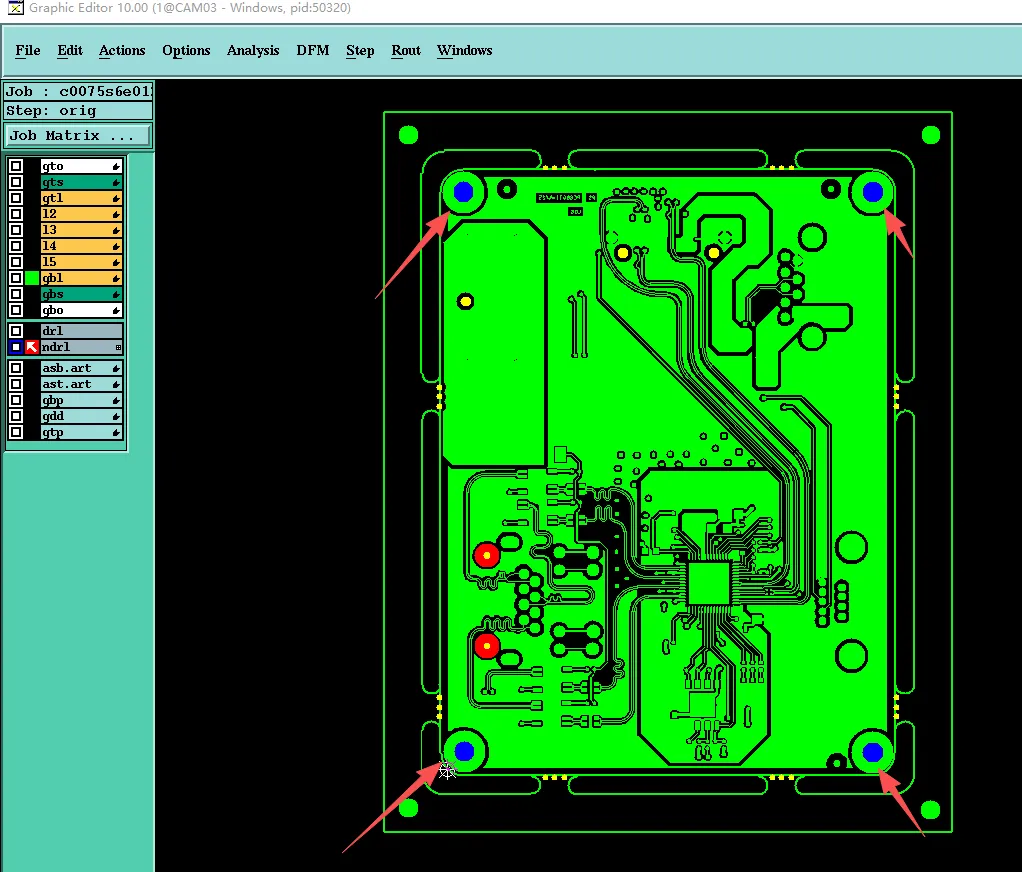
Figure 4: four 2.7mm NPTH holes had corresponding pads on the circuitry layers
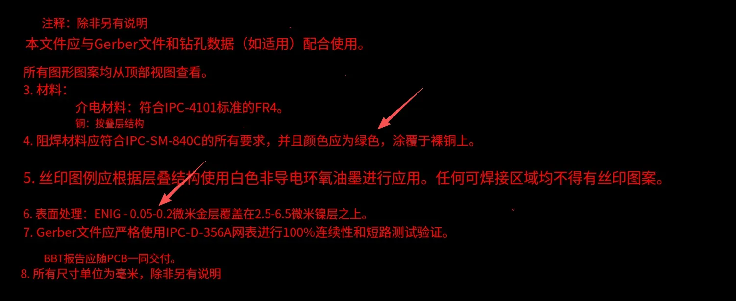
Figure 5: conflicts between the documentation and actual files regarding ink color, ENIG thickness
We identified these during file cross-checking. Incorrect hole plating on NPTH features could cause unintended electrical connections or assembly problems. The customer confirmed non-plated treatment and allowed us to ignore conflicting reference files.
Manufacturing Risks and DFM Insights
This case highlights recurring DFM challenges in 6-layer designs with 2oz outer copper: inconsistent via mask specifications, overly optimistic solder mask bridge expectations in fine-pitch areas, and documentation mismatches. Designers frequently underestimate the impact of copper weight on final feature spacing and via treatment in BGA/IC zones.
If these issues are ignored, typical consequences include solder shorts, open circuits, assembly failures, impedance deviation, and reduced yield. In similar projects, unconfirmed via openings in dense areas led to significant SMT rework and delays.
How the Engineering Team Resolved the Issues
Our CAM team provided marked-up images clearly showing the via mask inconsistencies and tight spacing areas. We suggested specific handling for NPTH holes and received approval for standard mask bridge limitations. We noticed the documentation conflicts early and confirmed which files took priority.
For UL markings, we added available information and confirmed with the customer. All production files were updated after feedback, ensuring clean manufacturing data and reduced risk.
Final Manufacturing Outcome
All engineering questions were resolved through customer confirmation. Production files were adjusted for consistent via treatment, accepted no-bridge conditions in tight areas, confirmed NPTH holes, and aligned documentation. The order was successfully released for production.
Key Takeaways for PCB Designers
- Clearly specify via solder mask treatment (open or covered) for every via, especially in dense IC/BGA regions.
- Account for solder mask compensation and copper weight when designing fine-pitch IC pad spacing to ensure reliable mask bridges.
- Explicitly define NPTH holes even when pads are present to avoid unintended plating.
- Ensure all fabrication notes, stackup files, and Gerber data are consistent and up-to-date.
- Provide complete UL marking details (including batch information) or allow factory standard practices.
- Review large openings for resin plugging requirements to prevent solder wicking issues.
- Allow reasonable DFM optimizations for solder mask bridges in tight areas.
FAQ
Q1: Why is via solder mask treatment important in dense areas?
A1: Inconsistent treatment can cause solder wicking into vias or insufficient bridging between pads, leading to shorts or open circuits during assembly.
Q2: What happens with tight pad spacing after compensation?
A2: Solder mask bridges may fail, increasing the risk of solder shorts between pads. Confirming no-bridge acceptance prevents assembly defects.
Q3: Should NPTH holes have pads?
A3: Pads are acceptable for mechanical support, but the holes must be clearly specified as non-plated to prevent copper plating inside them.
Q4: Why do factories sometimes ignore certain reference files?
A4: When files conflict or contain outdated information, the factory confirms the authoritative data to avoid manufacturing errors based on incorrect specs.
Q5: How does 2oz outer copper affect solder mask design?
A5: It requires more compensation, reducing effective spacing and making solder mask bridges harder to achieve in fine-pitch areas.