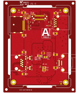
6 Layer FR4 PCB Production Record #FR4-20260403-018
| Parameter | Value | Parameter | Value |
|---|---|---|---|
| PCB Type | FR4 PCB | Quantity | 20 pcs |
| Layers | 6 Layers | Board Type | Panel PCB |
| Dimensions | 95 x 75 mm | Copper Weight | 2oz |
| Thickness | 2 mm | Min Track / Spacing | 4/4mil |
| Surface Finish | ENIG (Immersion Gold) | Min Hole Size | 0.2mm |
| Solder Mask | Red | Silkscreen | White |
| Stack-up | Default | Impedance Control | Yes |
This 6-layer FR-4 board (95 × 75 mm, 2.0 mm finished thickness, KB-6165F material) was built as single-unit panels for a quantity of 20 pieces. It featured 1 oz outer copper and 2 oz inner layers, 4 mil minimum line/space, 0.2 mm minimum hole size, red solder mask, white legend, ENIG surface finish, and impedance control with 100% flying probe testing. Resin plugging was applied to specified vias, along with routed slots and mechanical forming.
DFM review addressed several mask and process clarifications. Via openings showed inconsistency in the data, with some requiring open windows and others tented with solder mask. NPTH holes with associated pads were confirmed for non-plated processing. Tight trace spacing after compensation (0.09 mm) prevented reliable solder mask bridges in IC areas; customer acceptance of bridge loss was confirmed. Additional resolutions included confirmation of ink color and gold thickness alignment, large via window resin plugging requirements, and waivers for non-referencable stackup documentation and certain UL/batch marking details. via mask inconsistency and tight solder mask bridge handling followed standard engineering verification.
All engineering questions received customer confirmation prior to production release. The order completed within the 9-day delivery window. Final electrical testing, impedance verification, and quality documentation confirmed compliance with the approved parameters and processes.
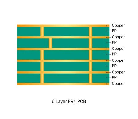
Six layer FR4 boards provide optimized routing density and power distribution. They require precise lamination and plating process control to maintain yield and reliability.

In-depth guide to the most frequent Engineering Queries (EQ) and DFM issues in Multilayer FR4 PCB (4/6/8+ layers) production. Real factory insights on stack-up confirmation, impedance control, copper balance, inner layer design, via treatment, registration, and practical prevention strategies.
| Order ID | PCB Type | Layers | Dimensions | Solder Mask | Surface Finish | Quantity | Action |
|---|---|---|---|---|---|---|---|
| FR4-20260520-046 | FR4 PCB | 2 | 94.21 x 275 | Green | ENIG (Immersion Gold) | 75 | View detail |
| FR4-20260515-068 | FR4 PCB | 14 | 244 x 267 | Green | ENIG (Immersion Gold) | 10 | View detail |
| FR4-20260506-017 | FR4 PCB | 6 | 55 x 41.7 | Green | ENIG (Immersion Gold) | 15 | View detail |


