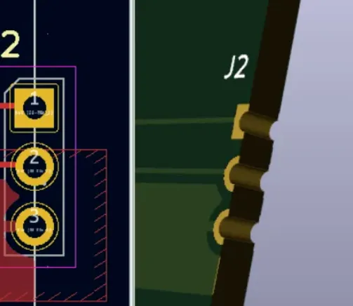
Poor via design is one of the most common reasons boards fail DFM review or show reliability problems after assembly. Vias that look fine in the PCB editor can create plating voids, drill breakout, signal reflections, or thermal hotspots once the board reaches the fabricator. Getting via type, size, clearance, and placement right in KiCad directly determines whether the design can be manufactured reliably and at reasonable cost.
This article covers the main via types used in modern PCBs, how to set proper via rules inside KiCad, size selection guidelines for standard and HDI boards, placement practices for signal, power, and thermal needs, and the manufacturing problems that appear when those rules are ignored. The goal is practical: finish a design that passes DRC, produces clean Gerbers and drill files, and survives fabrication and assembly without redesign.
Understanding PCB Via Types
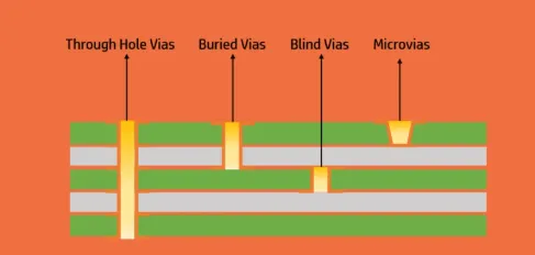
Vias are the vertical interconnects that connect copper layers. The type you choose affects layer count, fabrication process, cost, and reliability.
Through-hole vias These go from the top layer all the way through the board to the bottom layer. They are drilled after lamination and plated through. Through-hole vias are the default choice for most 2–8 layer boards because every fabricator can make them and the process is well controlled. They consume space on every layer, so they are less suitable for very dense designs.
Blind vias A blind via connects an outer layer to one or more inner layers but does not go all the way through the board. Fabricators create them by controlled-depth drilling or sequential lamination. Blind vias free up routing space on the opposite side of the board and are common in HDI and high-layer-count designs. They increase cost and require tighter process control.
Buried vias Buried vias connect only inner layers and never reach the outer surfaces. They are formed during sequential build-up and then covered by subsequent layers. Buried vias give the densest routing but add significant cost and fabrication complexity. Most standard PCB houses do not offer them on quick-turn service.
Microvias Microvias are laser-drilled holes, typically ≤0.15 mm diameter, that connect adjacent layers (or span a very short distance). They are the foundation of HDI stack-ups. Microvias can be stacked or staggered. Because they are laser-formed rather than mechanically drilled, aspect-ratio limits are much lower and plating quality is usually better when the design follows manufacturer guidelines.
Creating Via Rules in KiCad
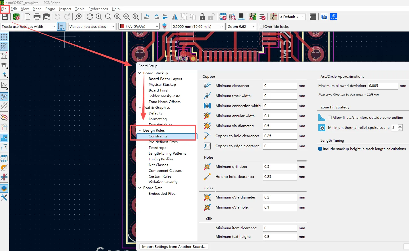
KiCad manages vias through the Board Setup → Design Rules → Constraints and the Net Classes / Custom Rules system. Setting these correctly before routing prevents most later manufacturing rejects.
Via size settings
In Board Setup → Design Rules → Constraints you define the minimum via diameter and minimum via drill. These values become the floor for every via you place. For most FR-4 boards with 1 oz copper, a practical starting point is:
- Minimum via diameter: 0.6 mm
- Minimum via drill: 0.3 mm
You can create tighter rules for specific net classes (for example high-speed differential pairs or power nets) using custom design rules.
Drill diameter
The drill size determines the finished hole after plating. Fabricators typically plate 20–25 µm of copper in the barrel. If your design rule allows a 0.25 mm drill on a standard mechanical process, many shops will reject it or force a process change. Always leave margin: specify a finished hole size that the fabricator's minimum mechanical drill can achieve with reliable plating.
Clearance requirements
Via-to-via, via-to-track, and via-to-pad clearances must satisfy both electrical and manufacturing needs. Insufficient annular ring is one of the most frequent DFM failures. KiCad's DRC checks the annular ring against the values you set in Constraints. A safe starting annular ring for standard through-hole vias is 0.15 mm (0.006 in). For microvias the annular ring can be smaller, but only if the fabricator's laser process supports it.
After setting the rules, run a full DRC. Any via that violates minimum size, annular ring, or clearance will be flagged before you generate manufacturing files.
Choosing the Right Via Size
Standard PCB vias
For 2–6 layer boards running ordinary digital and power signals, 0.6 mm pad / 0.3 mm drill (or 0.8 mm / 0.4 mm for higher current) remains the most manufacturable choice. These sizes give good plating yield, adequate annular ring even with moderate registration error, and low cost.
High-density PCB requirements
When component pitch drops below 0.5 mm or routing channels become tight, designers move to 0.45–0.5 mm pad / 0.2–0.25 mm drill. At this point you must confirm that the chosen fabricator supports the drill size and can maintain annular ring under their registration tolerance.
HDI considerations
HDI boards rely on microvias (usually 0.1–0.15 mm laser drill). Stacked microvias require filled and planarized vias so the next laser drill lands on a flat surface. Aspect ratio for microvias is typically kept ≤0.8:1. Exceeding the fabricator's microvia aspect-ratio limit produces incomplete plating and open circuits after thermal cycling.
Always match the via size to both the electrical need and the process capability of the board house that will build the design. A via that passes KiCad DRC but violates the fabricator's capability table will still be rejected at DFM.
Via Placement Best Practices
Signal routing
Keep vias in high-speed nets to a minimum. Every via introduces a small impedance discontinuity and stub. When a via is required, place it close to the component pad and use the shortest possible stub (or back-drill if the stack-up allows). For differential pairs, keep the via pattern symmetric and maintain consistent via-to-via spacing so the differential impedance stays controlled.
Thermal vias
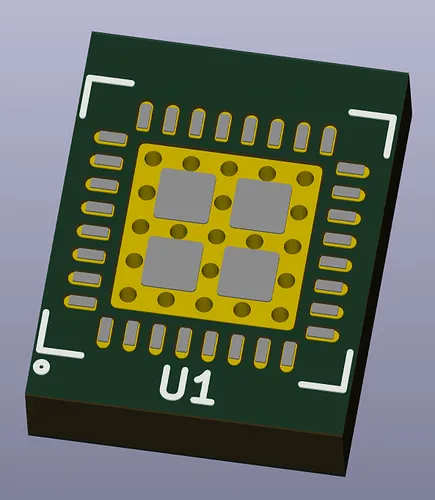
Under power devices or LED pads, an array of thermal vias transfers heat to inner copper planes or to a heat sink on the opposite side. Typical thermal via size is 0.3–0.4 mm drill with 0.6–0.7 mm pad. Fill the vias with conductive or non-conductive epoxy if the design requires a flat surface for soldering or underfill. Unfilled thermal vias can create solder voids during reflow.
Power distribution
Power vias should be sized for current. A single 0.3 mm drill via can carry roughly 1–1.5 A depending on copper weight and temperature rise. For higher current, use multiple vias in parallel and connect them to solid copper pours on adjacent layers. Place power vias near the source and load pins rather than at the far end of a long power trace.
In all cases, keep vias away from board edges and from areas that will be scored or routed, because edge clearance rules still apply after plating.
Common Via Design Problems
Insufficient clearance
When via-to-track or via-to-via clearance is set too tight, the fabricator's etch and registration tolerances produce shorts or reduced insulation. KiCad DRC will catch most of these if the clearance rules are realistic. The remaining risk appears when the design uses different net classes with conflicting clearance values that were never verified together.
Poor manufacturability
Aspect ratios above 8:1–10:1 for mechanical vias often result in incomplete plating. Microvias with excessive depth or stacked vias without proper fill create voids that open after thermal cycling. Blind and buried vias that do not follow the fabricator's sequential-lamination rules force the board house to reject the job or quote a much higher price.
Reliability risks
Thin annular rings crack under thermal stress. Unfilled vias under BGA pads can collect flux residue or create solder wicking. Vias placed too close to the edge of a copper plane can cause plane resonance or EMI issues. All of these problems are visible only after the board is built and tested; catching them in KiCad with proper rules and a final DFM-oriented review is far cheaper.
After routing is complete, generate Gerbers, the Excellon drill file, and the IPC-356 netlist. Open the Gerbers in a viewer and confirm that every via has the expected annular ring and that no drill hits a plane without a proper clearance. Then submit the package for DFM review.
After completing the KiCad design process and generating the manufacturing files, engineers can upload the Gerbers, drill files, and stack-up information to AIVON for PCB fabrication and assembly. AIVON's DFM checks catch many via-related issues (annular ring, aspect ratio, minimum drill) before production starts, reducing the chance of a respinned board.
FAQ
Q1: What is the minimum via size I can use in KiCad for a standard 4-layer board?
A1: For most fabricators a 0.6 mm pad with 0.3 mm drill is safe. Smaller sizes are possible but must be confirmed against the board house's capability table; otherwise the design may fail DFM even if KiCad DRC passes.
Q2: How do I set different via sizes for power nets and signal nets in KiCad?
A2: Create separate net classes, assign the nets, then use custom design rules (Board Setup → Design Rules → Custom Rules) to apply larger via diameter and drill values only to the power class. Run DRC afterward to verify both sets of rules.
Q3: Can I use blind and buried vias in a normal KiCad project?
A3: Yes. Define the via type in the via properties or by using the appropriate layer pair when placing the via. The limitation is not KiCad; it is whether your chosen fabricator supports sequential lamination and the associated cost and lead time.
Q4: Why do my thermal vias cause solder voids during assembly?
A4: Unfilled vias under a thermal pad allow solder to wick into the hole. Specify filled and capped (or tented) vias in the fabrication notes, or use a via-in-pad process that the assembler supports.
Q5: How does via design affect the Gerber and drill files I send for manufacturing?
A5: KiCad exports the via pads into the copper Gerber layers and the drill sizes into the Excellon file. Incorrect via rules produce wrong annular rings or illegal drill sizes that the fabricator will flag during DFM. Always review the generated files before ordering.