Many boards fail to meet performance targets or incur unexpected cost increases because the layer stackup was chosen late—or chosen without reference to what the manufacturer can actually build. Signal integrity problems, impedance mismatches, excessive warpage, or higher fabrication prices often trace back to a stackup that looked fine in KiCad but did not match real process capabilities or material availability.
This guide explains how to plan PCB stackups in KiCad with manufacturing requirements in mind. You will learn the function of each layer type, how to configure layers correctly, which common configurations work for most projects, what high-speed designs demand, and how to collaborate with fabricators so the stackup you design is the stackup that can be produced reliably and cost-effectively.
Why PCB Stackup Design Affects Performance and Cost
The stackup defines the order and type of copper and dielectric layers, copper weights, dielectric thicknesses, and overall board thickness. It directly controls impedance, return-path quality, power-delivery performance, electromagnetic shielding, mechanical stability, and fabrication cost.
A poorly chosen stackup can force the use of more expensive materials, tighter process controls, or additional layers that the design did not truly need. Conversely, a stackup planned early and matched to the manufacturer's standard offerings usually delivers better electrical performance at lower cost.
Understanding PCB Layer Structure
Signal Layers
These carry the majority of routing. Outer signal layers are easier to modify but more exposed to EMI; inner signal layers benefit from adjacent reference planes.
Power Layers
Solid or segmented copper planes that distribute power. They reduce voltage drop and provide low-impedance paths when properly decoupled.
Ground Layers
Unbroken ground planes are the foundation of good signal integrity. They supply continuous return paths and act as shields between signal layers.
Dielectric Layers
The insulating material (usually FR-4 or higher-performance laminates) between copper layers. Thickness and dielectric constant (Dk) determine impedance and overall board thickness.
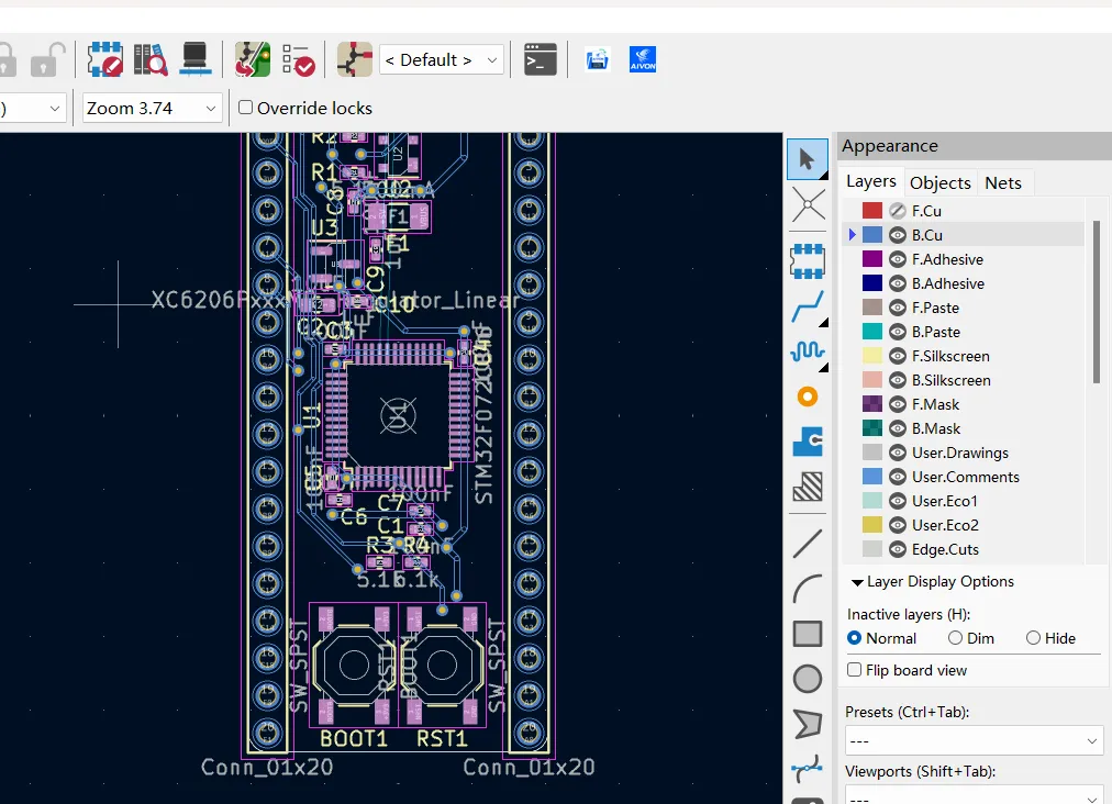
In KiCad these layers appear in the Layer Manager and are reflected in the board stackup that will later be communicated to the manufacturer.
Setting Up Layers in KiCad
Layer Manager Overview
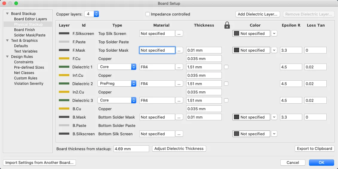
Open Board Setup → Physical Stackup (or Layers in older versions). Here you define the number of copper layers, their names, and the dielectric materials between them. KiCad allows you to set approximate thicknesses and copper weights so that impedance calculations and 3D views remain realistic.
Assigning Copper Layers
Name layers clearly (F.Cu, In1.Cu, In2.Cu, B.Cu, etc.). Assign the correct type (signal, power, mixed) so that the design-rule system and zone tools behave as expected. Enable only the layers you will actually use; unused layers still affect the manufacturer's pricing if they are left in the stackup definition.
Defining Board Structure
Enter the intended overall thickness and copper weights. Add a text note or fabrication drawing that records the full stackup (layer order, copper weight, dielectric type and thickness, surface finish). This note travels with the design and prevents ambiguity when the board reaches the fab.
Practical guidance: decide the layer count and approximate stackup before placement begins. Changing the number of layers after routing is expensive in both time and risk.
Common PCB Stackup Configurations
2-Layer PCB Stackup
Top signal / Bottom signal (with ground pours). Suitable for simple, low-speed designs. Cost is lowest, but controlled impedance and clean return paths are harder to achieve. Keep sensitive signals short and use a solid ground pour on the bottom layer.
4-Layer PCB Stackup
A widely used production stackup is:
- Top signal
- Ground plane
- Power plane
- Bottom signal
This arrangement gives every signal layer an adjacent reference plane, improves EMI performance, and remains cost-effective for most commercial products. Alternative 4-layer arrangements (signal-ground-signal-power) are also common when power distribution needs are lighter.
Multilayer PCB Stackup
Six-layer and higher boards add extra signal or plane layers. Typical goals are tighter impedance control, additional routing density, or better power integrity. Each added layer increases cost and can affect lead time, so justify every extra layer with a clear electrical or density requirement.
Manufacturing perspective: standard 2-layer and 4-layer constructions are stocked by most fabricators and therefore cheaper and faster. Non-standard layer counts or unusual dielectric thicknesses often require special material orders and raise both price and risk.
Stackup Considerations for High-Speed Designs
Controlled Impedance
When traces must meet a target impedance (50 Ω single-ended, 90–100 Ω differential, etc.), the stackup dielectric thickness, copper weight, and trace geometry must be calculated together. Enter the intended dielectric constants and thicknesses in KiCad so that the impedance calculator or external tools produce realistic results.
Signal Reference Planes
High-speed signals should reference a continuous ground (or sometimes power) plane on an adjacent layer. Avoid changing reference planes without stitching vias; otherwise return currents are forced to detour and radiation increases.
Differential Pairs
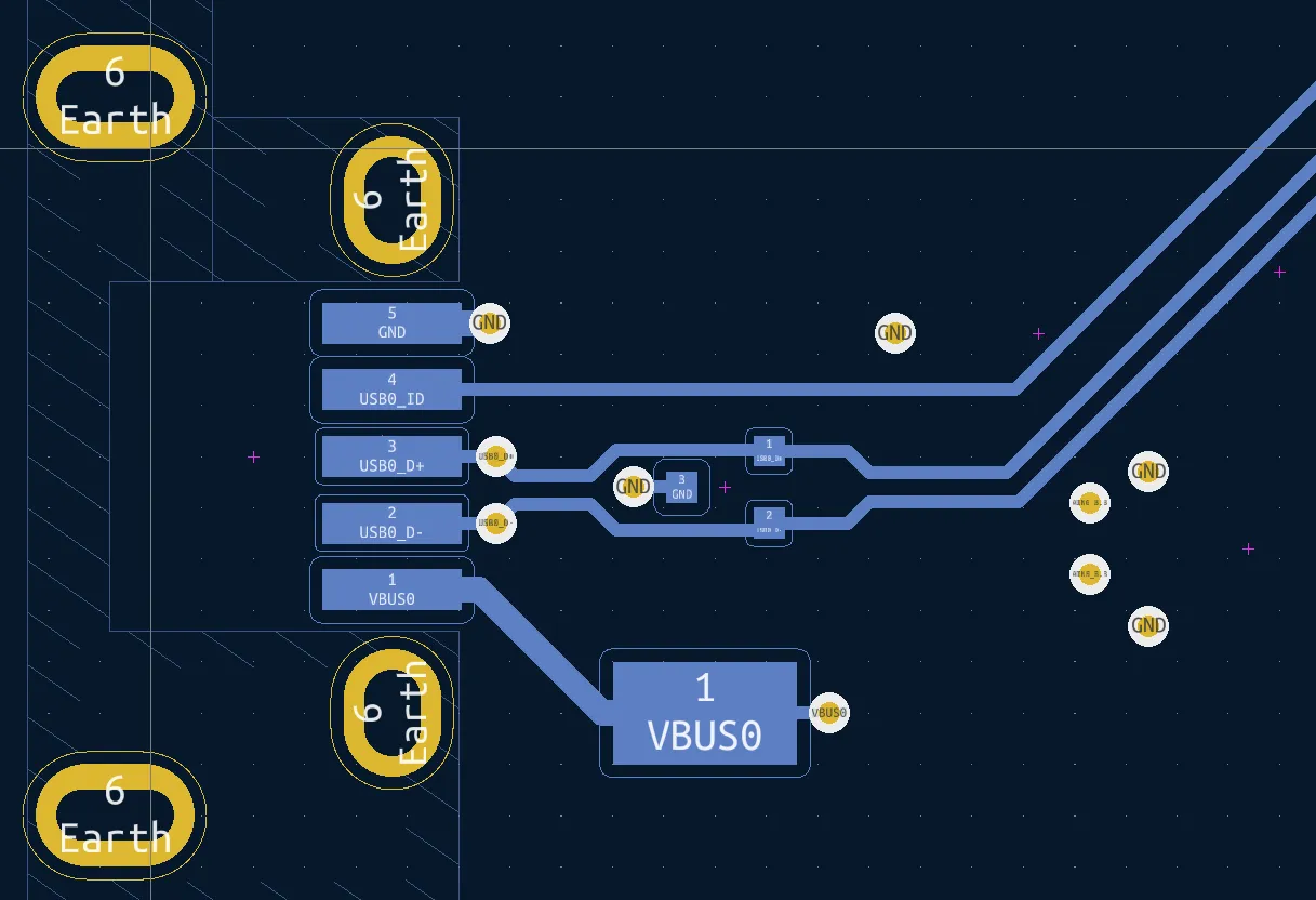
Route differential pairs over a continuous reference plane and keep the pair tightly coupled. The stackup must provide consistent dielectric height so that the calculated differential impedance remains valid across the board.
Manufacturing Considerations
Copper Thickness
Standard outer-layer copper is 1 oz (35 µm); inner layers are often 0.5 oz or 1 oz. Heavier copper improves current capacity but reduces the ability to etch fine traces and can increase cost.
Material Selection
FR-4 is the default for most designs. Higher-speed or higher-frequency boards may need lower-loss laminates (lower Df). Confirm material availability and cost with the manufacturer before locking the stackup.
Fabrication Limitations
Minimum core and prepreg thicknesses, maximum aspect ratio, and registration accuracy limit how thin or how complex a stackup can be. Extremely thin dielectrics or very thick boards may fall outside a given fab's process window.
Always design the stackup inside the manufacturer's published capabilities rather than assuming any construction is possible.
Working with PCB Manufacturers on Stackup Design
Share the intended stackup early—ideally while the schematic is still being finished. Most fabricators can provide a recommended stackup that meets your impedance and thickness targets using materials they regularly stock. This avoids late redesigns and unexpected cost increases.
When the design is complete, include the final stackup note in the fabrication package. Clear communication of layer order, copper weights, dielectric materials, and overall thickness is one of the simplest ways to prevent manufacturing misunderstandings.
Engineers who plan the stackup in KiCad with real process limits in mind, then confirm it with the manufacturer, consistently achieve better electrical performance and fewer production surprises. The stackup is not merely a KiCad setting—it is the foundation that links design intent to a board that can be built reliably and economically.
FAQ
Q1: How do I set up a PCB stackup in KiCad?
A1: Open Board Setup → Physical Stackup, define the number of copper layers, assign names and types, enter copper weights and dielectric thicknesses, and add a clear stackup note for the manufacturer.
Q2: What is the most common 4-layer PCB stackup for KiCad designs?
A2: Top signal – Ground plane – Power plane – Bottom signal. This configuration gives both signal layers an adjacent reference plane and is widely supported by manufacturers at reasonable cost.
Q3: When should I choose a 4-layer board instead of a 2-layer board?
A3: Choose 4-layer when you need better signal integrity, controlled impedance, cleaner power distribution, or higher routing density. The modest cost increase is usually justified by improved performance and lower EMI.
Q4: How does PCB stackup affect controlled impedance in KiCad?
A4: Impedance depends on trace geometry, copper weight, and the dielectric thickness and constant between the signal layer and its reference plane. Accurate stackup data in KiCad (or in the manufacturer's calculator) is required for reliable impedance control.
Q5: Should I confirm the stackup with the manufacturer before finishing the layout?
A5: Yes. Early confirmation ensures the materials and thicknesses you plan are available, cost-effective, and within the fab's process limits, preventing late changes that force re-routing or re-design.