Introduction
High-Tg PCBs represent a critical advancement in printed circuit board technology, enabling reliable operation in demanding environments with elevated temperatures. These boards use laminates with a glass transition temperature typically exceeding 170 degrees Celsius, making them suitable for applications in automotive electronics, industrial controls, and aerospace systems. Via design plays a pivotal role in High-Tg PCB via design, as vias serve as essential interconnects between layers while enduring thermal stresses and mechanical strains. Poor via implementation can lead to failures like cracking or delamination, compromising overall board integrity. This guide explores the principles, best practices, and considerations for effective High-Tg PCB via design, tailored for electrical engineers seeking optimized performance. By focusing on key parameters such as size, placement, thermal management, and impedance, engineers can enhance reliability and signal integrity.
Understanding High-Tg PCBs and the Role of Vias
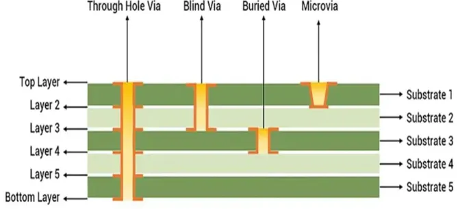
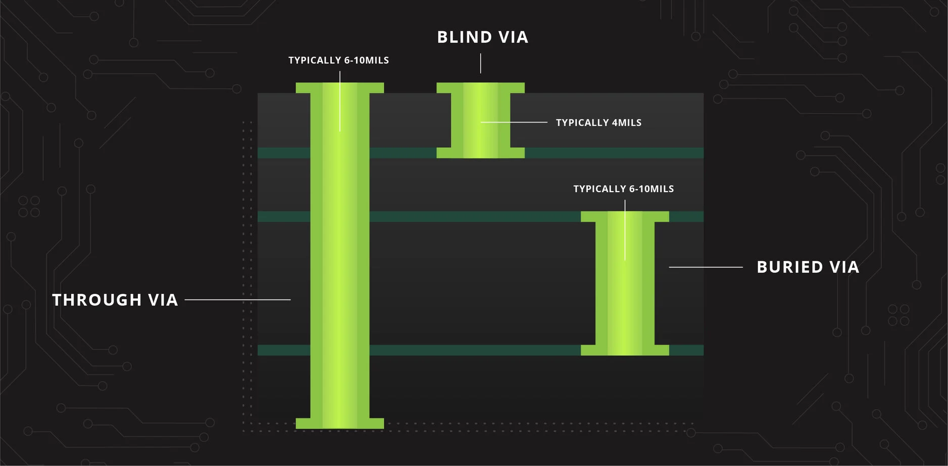
High-Tg PCBs employ resin systems that maintain mechanical stability above standard FR-4 limits, resisting deformation during soldering or operational heat. Vias in these boards are plated through-holes that facilitate vertical interconnections, categorized as through-hole, blind, or buried types. In High-Tg materials, the higher modulus of elasticity amplifies stresses at via interfaces due to coefficient of thermal expansion (CTE) mismatches between copper plating and the dielectric. This mismatch becomes pronounced during thermal cycling, potentially causing barrel cracking or interface separation. Electrical engineers must prioritize via reliability to meet performance demands in high-reliability applications. Standards like IPC-2221 provide foundational guidelines for via configuration to mitigate these risks.
The relevance of precise via design intensifies in multilayer High-Tg PCBs, where layer count increases via density and complexity. Blind and buried vias reduce board thickness and improve routing efficiency, but their fabrication demands tighter process controls in high-Tg laminates. Engineers evaluate via types based on stackup requirements, ensuring compatibility with drilling and plating processes. Ultimately, robust via design ensures signal propagation, power distribution, and thermal dissipation without compromising board lifespan.
Key Principles of High-Tg PCB Via Size
High-Tg PCB via size directly influences manufacturability, electrical performance, and thermal reliability. Via diameter, including drill size and finished hole size, must balance current-carrying capacity with aspect ratio limitations. In high-Tg materials, the stiffer laminate requires optimized plating thickness to prevent voids during electroless and electrolytic copper deposition. Engineers consider annular ring dimensions to maintain structural integrity under thermal expansion. Aspect ratios, typically limited to 10:1 or less per design guidelines, prevent plating inconsistencies that could lead to high-resistance paths.
Smaller vias enable higher density but increase fabrication challenges, such as drill wander in harder high-Tg resins. Larger vias accommodate higher currents but consume more board real estate, impacting routing. Electrical engineers simulate thermal and mechanical stresses to select via sizes that withstand reflow profiles and operational temperatures. Compliance with performance specifications outlined in IPC-6012 ensures vias meet qualification criteria for rigid boards. By methodically sizing vias, designs achieve optimal reliability without over-specification.
Strategic High-Tg PCB Via Placement
High-Tg PCB via placement affects signal integrity, mechanical stability, and heat distribution across the board. Vias positioned too closely risk drill breakout or insufficient copper spacing, exacerbating CTE-induced stresses. Engineers space vias according to clearance rules, considering voltage levels and environmental factors like humidity. Placement near board edges or corners demands reinforcement to counter warpage tendencies in high-Tg laminates during lamination or assembly.
Optimal placement aligns vias with component pads for shortest interconnect lengths, minimizing inductance in high-speed signals. In power planes, staggered via arrays distribute current evenly, reducing hotspots. Electrical engineers use stackup planning to avoid via stubs that degrade performance in multilayer configurations. Strategic placement also facilitates inspection and rework, enhancing yield in production. Thoughtful via placement integrates seamlessly with overall board topology for superior functionality.
High-Tg PCB Thermal Vias: Design and Implementation
High-Tg PCB thermal vias address heat dissipation challenges in power-intensive designs, channeling heat from components to inner planes or the opposite side. These vias, often filled or arrayed, provide low thermal resistance paths through the laminate. In high-Tg materials, the lower thermal conductivity necessitates denser via fields to compensate, as the stiff dielectric hinders lateral heat spreading. Engineers cluster thermal vias under hot components like power ICs or LEDs, ensuring plated walls maximize conduction.
Design involves calculating via pitch and count based on power dissipation and junction temperatures. Filled thermal vias, using conductive epoxy, prevent solder wicking during assembly while maintaining thermal efficacy. Arrays must avoid interfering with signal routing, requiring careful plane cutouts. Testing per IPC-TM-650 methods validates thermal performance under simulated loads. Effective High-Tg PCB thermal vias extend component life and prevent board-level failures.
Managing High-Tg PCB Via Impedance
High-Tg PCB via impedance control is crucial for high-frequency applications, where vias act as discontinuities introducing reflections and crosstalk. Via stubs from unused segments lengthen transition times, degrading eye diagrams. Backdrilling removes stubs, tailoring impedance to transmission line characteristics. In high-Tg dielectrics, which may exhibit slightly higher dissipation factors, via capacitance increases with diameter, necessitating precise sizing.
Engineers model via impedance using field solvers, targeting 50-ohm or 100-ohm matches depending on differential or single-ended lines. Controlled depth vias and optimized pad transitions minimize return loss. Material uniformity in high-Tg laminates supports consistent dielectric constants, aiding impedance stability. Integration with impedance-controlled traces ensures end-to-end performance. Mastering High-Tg PCB via impedance preserves signal quality in RF and gigabit designs.
Related Reading: Understanding High Tg PCB Impedance Control: A Practical Guide
Best Practices for High-Tg PCB Via Design
Adopt a systematic approach to High-Tg PCB via design by starting with stackup analysis to predict thermal and mechanical behaviors. Select via types based on layer access needs, favoring blind vias for inner layer efficiency. Maintain plating thickness per performance specs to endure cyclic stresses. Incorporate tenting on non-critical vias to protect against solder contamination.
Perform design rule checks for spacing, annular rings, and aspect ratios aligned with fabrication capabilities. Simulate thermal profiles to validate via arrays and power distribution. Prototype testing under accelerated conditions reveals weaknesses early. Collaborate with fabricators for design-for-manufacturability feedback. These practices yield robust, high-yield High-Tg PCBs.
Conclusion
Via design in High-Tg PCBs demands a holistic understanding of material properties, thermal dynamics, and electrical demands. Optimizing High-Tg PCB via size, placement, thermal vias, and impedance ensures reliability in harsh environments. Engineers benefit from structured adherence to standards, avoiding common pitfalls like cracking or signal degradation. Implementing these principles elevates design quality, supporting advanced applications. Future trends toward finer pitches will further emphasize precise via strategies.
FAQs
Q1: What factors determine optimal High-Tg PCB via size?
A1: High-Tg PCB via size depends on aspect ratio limits, current requirements, and plating uniformity to prevent voids in stiff laminates. Engineers balance density needs with manufacturability, ensuring annular rings withstand CTE stresses. Simulation tools aid in selecting sizes that maintain low resistance and thermal reliability without specifying exact dimensions. Adhering to IPC-2221 guidelines supports consistent performance across designs. (62 words)
Q2: How should vias be placed in High-Tg PCB designs for best results?
A2: In High-Tg PCB via placement, prioritize spacing to avoid breakout and stress concentrations, especially near edges. Align with pads for minimal inductance and stagger in power areas for even distribution. Consider stackup to eliminate stubs affecting signals. This approach enhances mechanical stability and routing efficiency in multilayer boards. (58 words)
Q3: What role do thermal vias play in High-Tg PCBs?
A3: High-Tg PCB thermal vias efficiently transfer heat through low-conductivity laminates, using arrays under components to reach inner planes. Filled designs prevent wicking while preserving conduction. Proper pitch and count counter the material's stiffness, validated through thermal testing. They are essential for power electronics reliability. (54 words)
Q4: How is via impedance controlled in High-Tg PCBs?
A4: High-Tg PCB via impedance management involves backdrilling stubs and optimizing pad geometries to match trace impedances. Model capacitance from via dimensions against dielectric properties. This minimizes reflections in high-speed signals, ensuring integrity. Uniform materials aid predictability. (52 words)
References
IPC-2221B — Generic Standard on Printed Board Design. IPC, 2003
IPC-6012F — Qualification and Performance Specification for Rigid Printed Boards. IPC, 2023
IPC-TM-650 — Test Methods Manual. IPC


