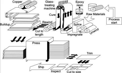
Help
  • FAQ
    browse most common questions
  • Live Chat
    talk with our online service
  • Email
    contact your dedicated sales:
0

PCB Manufacturing

PCB Back Drilling: The Key to Unlocking High Frequency Performance
signal integrity impedance control high frequency pcb pcb back drilling via stub reduction

PCB Back Drilling: The Key to Unlocking High Frequency Performance

PCB back drilling removes via stubs to enhance signal integrity in high-frequency PCB design. Benefits cover impedance control, reflection reduction, and crosstalk minimization for multilayer boards. Practical best practices and troubleshooting help engineers achieve reliable high-speed performance in telecom and servers.

The Future of HDI PCBs: Trends in Miniaturization, Materials, and Manufacturing
pcb manufacturing pcb materials signal integrity hdi pcb miniaturization

The Future of HDI PCBs: Trends in Miniaturization, Materials, and Manufacturing

HDI PCB technology trends center on miniaturization with fine lines and microvias alongside advanced materials HDI for high speed signals. Next generation HDI PCB leverage low loss dielectrics and laser manufacturing for compact reliable boards. Electrical engineers get insights into future PCB manufacturing shifts and best practices.

Sequential Lamination for RF and Microwave PCBs: Optimizing Performance in High Frequency Applications
high frequency pcb fabrication rf pcb controlled impedance sequential lamination

Sequential Lamination for RF and Microwave PCBs: Optimizing Performance in High Frequency Applications

Sequential lamination refines RF PCB lamination and microwave PCB fabrication for high-frequency boards. It delivers precise via control, stable impedance, and low-loss materials to support telecom and radar systems. Factory practices address warpage, CTE mismatches, and layer buildup for reliable results in demanding applications. (197 characters)


2026 AIVON.COM All Rights Reserved
Intellectual Property Rights | Terms of Service | Privacy Policy | Refund Policy