Introduction
High-speed printed circuit boards operate at frequencies exceeding several gigahertz, where signal integrity becomes a critical concern for reliable performance. Traditional testing methods often fall short in detecting subtle issues like impedance mismatches or crosstalk in these environments. Design for testability, or DFT, integrates specific features into the PCB layout to enable thorough signal integrity testing without compromising functionality. High speed PCB DFT ensures that engineers can verify key parameters such as transmission line integrity and high frequency response during manufacturing and assembly stages. By incorporating DFT early in the design process, teams reduce debug time and improve yield rates for complex multilayer boards. This approach aligns with industry needs for robust verification in applications like telecommunications and data centers.
Signal integrity testing in high-speed designs demands precision, as even minor discontinuities can lead to bit errors or timing violations. DFT facilitates access points for tools like time domain reflectometry, making high frequency testing more efficient. Engineers must balance test feature placement with signal performance to avoid introducing new integrity issues. Ultimately, effective DFT bridges design intent with manufacturable testability, ensuring boards meet operational demands.
What Is DFT in High-Speed PCBs and Why It Matters
Design for testability refers to intentional hardware modifications that simplify fault detection and performance validation on assembled boards. In high-speed PCBs, DFT extends beyond basic continuity checks to include provisions for signal integrity testing, such as dedicated probe points and scan chains. These elements allow non-invasive assessment of high frequency signals, where skin effect and dielectric losses dominate behavior. IPC-2221 outlines generic requirements for such design practices, emphasizing testability alongside reliability.
The relevance of high speed PCB DFT stems from the limitations of conventional in-circuit testing at multi-gigabit speeds. Probes and fixtures can introduce parasitic capacitance, distorting measurements and masking true signal behavior. DFT mitigates this by providing controlled access paths that preserve impedance profiles. For electric engineers, this means faster iteration cycles and higher confidence in prototypes transitioning to production.
Without DFT, signal integrity issues often surface late, during system-level integration, leading to costly respins. High frequency testing requires repeatable conditions, which DFT standardizes through features like boundary scan compatibility. Procurement teams also benefit, as DFT-enhanced boards yield better test coverage and reduced field failures. In essence, DFT transforms testability from an afterthought into a core design pillar.
Technical Principles Behind DFT for Signal Integrity
Signal propagation in high-speed PCBs follows transmission line theory, where characteristic impedance must remain consistent to minimize reflections. Discontinuities from vias, bends, or pads cause voltage standing wave ratios that degrade eye patterns. Impedance control forms the foundation of signal integrity, with DFT incorporating verification structures like matched-length daisy chains to monitor these effects across the board.
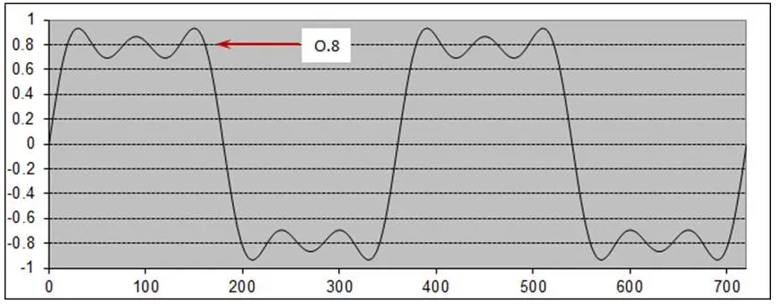
Time domain reflectometry, or TDR testing, exploits reflection coefficients to map impedance variations along traces. A step pulse travels the line, and echoes reveal mismatches with resolution down to millimeters. DFT supports TDR by placing low-parasitic launch points away from sensitive nets, ensuring accurate high frequency testing up to tens of gigahertz. Engineers analyze TDR waveforms for step heights corresponding to impedance steps, correlating them to layout features.
Crosstalk and insertion loss represent additional challenges, amplified by tight routing densities in high-speed designs. DFT employs guard traces or shielding vias around test nets to isolate measurements, preserving signal-to-noise ratios. High frequency testing via vector network analyzers complements TDR by providing S-parameter data, including return loss and insertion loss. These principles ensure DFT features do not degrade overall board performance but enhance diagnostic capability.
Dielectric material properties influence loss tangent at microwave frequencies, necessitating test coupons embedded in panels for material validation. IPC/TM-650 provides methods for such characterizations, guiding DFT implementation. By aligning test structures with production stackups, engineers validate models against fabricated realities.
Best Practices for Implementing DFT in High-Speed PCBs
Start with strategic test point placement, positioning them at line ends or critical junctions while maintaining minimum spacing to adjacent signals. Use 0.5 mm diameter pads on 1 mm pitch for flying probe compatibility, avoiding encroachment on high-speed routing channels. Impedance control remains paramount, so route test traces with identical width, length tolerance, and reference plane proximity as signal lines. This practice enables direct correlation between test results and functional performance.
Incorporate boundary scan chains per IEEE 1149.1 for digital nets, chaining high-speed I/Os where possible without altering timing budgets. For analog signals, add series resistors or attenuators at DFT access to dampen reflections during probing. Verify all DFT elements through simulation, modeling probe interactions to predict measurement fidelity. Regular design reviews catch potential conflicts early.
Dedicate panel coupons for TDR and VNA testing, including microstrip, stripline, and via transitions representative of the board. IPC-9252 specifies requirements for electrical testing of unpopulated boards, informing DFT fixture design. Calibrate test equipment to substrate Dk and Er values for precise de-embedding. Post-assembly, combine DFT with flying probe for hybrid signal integrity testing.
Layer stackup planning integrates DFT by reserving inner layers for ground returns under test lines, minimizing loop inductance. Avoid splitting planes under high-speed test segments to prevent resonance modes. Document DFT nets in netlists with unique naming for automated test program generation. These steps yield comprehensive coverage while upholding signal integrity.
Common Challenges and Troubleshooting in High-Speed DFT
Test points can inadvertently couple noise into adjacent high-speed lines if spacing falls below 3H rules, where H is trace height. Mitigate by enclosing points in ground via fences and simulating near-end/far-end crosstalk. Fixture parasitics often skew TDR results at frequencies above 10 GHz, requiring de-skew algorithms or air coplanar probes.
High frequency testing reveals via stub resonances not evident in lower-speed validation. Stub shortening or back-drilling, verified via DFT vias, resolves these. IPC-6012D sets performance benchmarks for rigid boards, aiding threshold decisions. Troubleshooting logs from DFT data accelerate root cause analysis, distinguishing fab variations from design flaws.
Conclusion
DFT in high-speed PCBs directly addresses signal integrity and testability by embedding verification features that withstand manufacturing variances. Key practices like impedance-controlled test traces and precise TDR access points enable reliable high frequency testing. Engineers gain actionable insights, reducing risks in dense, multilayer designs. Adhering to standards ensures consistency across the supply chain. Prioritizing high speed PCB DFT yields boards that perform predictably from prototype to deployment.
FAQs
Q1: What role does impedance control play in high speed PCB DFT?
A1: Impedance control maintains consistent characteristic values along traces, essential for minimizing reflections during signal integrity testing. DFT incorporates matched test structures to verify this control via TDR testing, detecting discontinuities early. Engineers route DFT nets identically to signals, ensuring representative measurements. This practice aligns with design rules, preventing signal degradation in high frequency environments.
Q2: How does TDR testing integrate with high speed PCB DFT?
A2: TDR testing uses time domain pulses to profile impedance profiles, with DFT providing low-distortion launch points for accuracy. Test vias and pads enable precise measurements without disassembling boards. In high frequency testing, TDR reveals via transitions and bends that affect signal integrity. Troubleshooting relies on DFT waveforms to pinpoint fixes like back-drilling.
Q3: Why is signal integrity testing critical in high-speed PCB manufacturing?
A3: Signal integrity testing validates propagation characteristics at gigabit speeds, where losses and crosstalk dominate. High speed PCB DFT facilitates this through accessible nets for probes and analyzers. Without it, latent defects escape detection, risking system failures. Best practices include panel coupons for baseline comparisons.
Q4: What are best practices for test point placement in DFT for impedance control?
A4: Place test points at trace ends with 1 mm minimum pitch, surrounded by ground vias for shielding. Maintain impedance matching by using same stackup references as signals. Simulate probe capacitance impacts pre-layout. This ensures high frequency testing fidelity without compromising nearby signal integrity.
References
IPC-2221C — Generic Standard on Printed Board Design. IPC, 2023
IPC-9252 — Requirements for Electrical Testing of Unpopulated Printed Boards. IPC, 2016
IPC-6012D — Qualification and Performance Specification for Rigid Printed Boards. IPC, 2015
IPC/TM-650 — Test Methods Manual. IPC