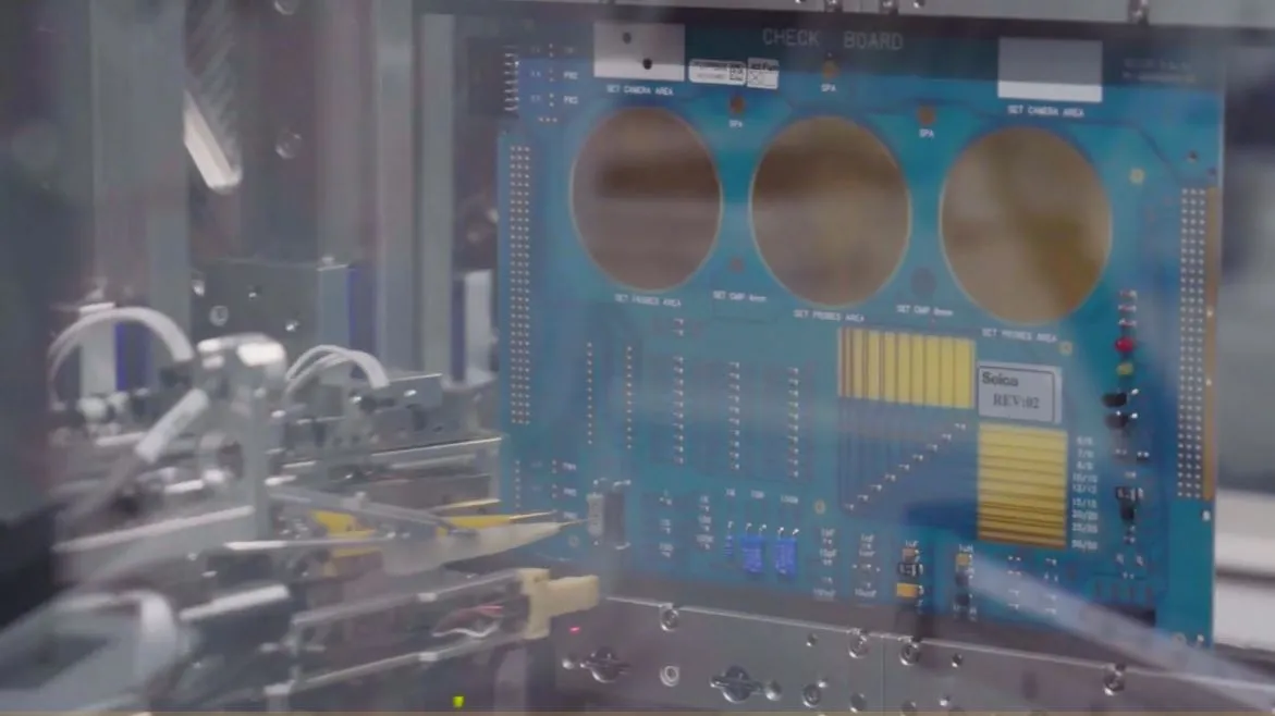
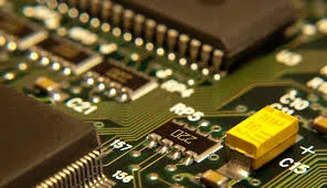
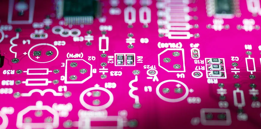
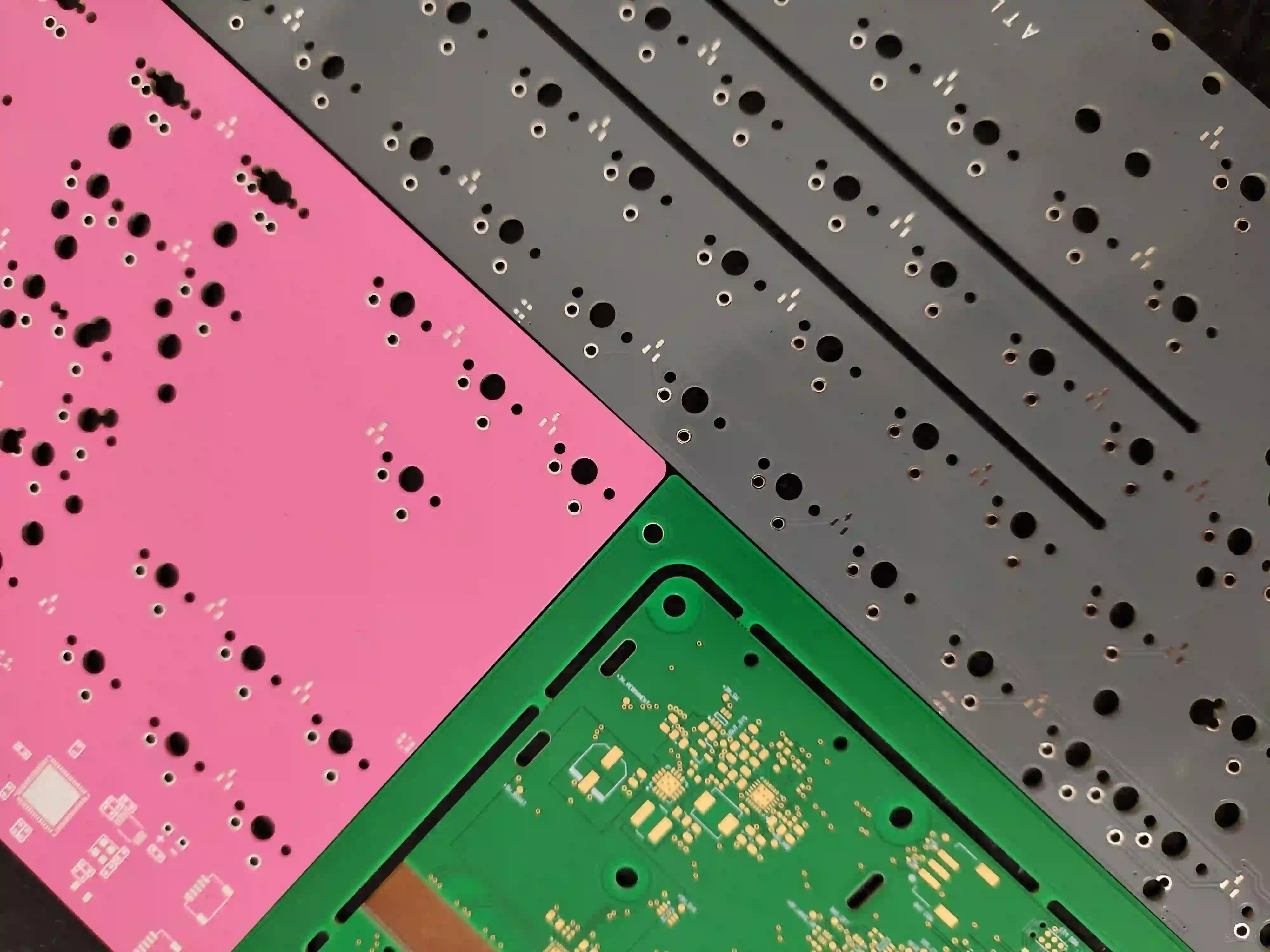
Help
  • FAQ
    browse most common questions
  • Live Chat
    talk with our online service
  • Email
    contact your dedicated sales:
0

PCB Manufacturing

PCB Gold Finger Design Rules: Avoiding Common Pitfalls for Reliable Connections
pcb reliability pcb design design best practices design rules gold fingers

PCB Gold Finger Design Rules: Avoiding Common Pitfalls for Reliable Connections

PCB gold finger design rules address spacing, length, alignment, chamfer, keepout areas for gold fingers, and plated through holes near gold fingers. Avoid pitfalls like misalignment and plating defects for reliable edge connectors. Practical tips help electric engineers ensure durable performance in high cycle applications.

PCB Direct Imaging: Overcoming Challenges with Warped or Uneven Substrates
pcb warpage pcb manufacturing laser direct imaging substrate flatness ldi solutions

PCB Direct Imaging: Overcoming Challenges with Warped or Uneven Substrates

Warped substrates disrupt PCB direct imaging by causing focus errors and yield drops in LDI processes. Apply vacuum fixturing, dynamic focusing, and lamination controls to flatten panels and ensure precise exposure. Tackle PCB manufacturing challenges with standards-based practices for better results and higher throughput.


2026 AIVON.COM All Rights Reserved
Intellectual Property Rights | Terms of Service | Privacy Policy | Refund Policy