Introduction
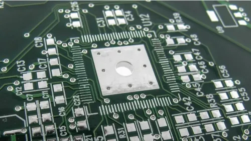
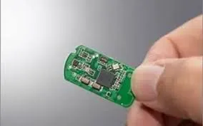
Electronics continue to shrink, driven by demands for portable devices, wearables, and IoT systems. This miniaturization pushes printed circuit boards toward higher densities with micro-components such as 01005 resistors and capacitors, fine-pitch BGAs, and 0.3 mm pitch QFNs. In-circuit testing, or ICT, plays a critical role in verifying these assemblies by electrically probing components for correct values, solder joint integrity, and continuity. However, testing miniaturized PCBs introduces unique hurdles, including limited probe access and alignment precision. Traditional bed-of-nails fixtures struggle with tight geometries, prompting shifts toward advanced ICT probe technology. Engineers must address these SMT ICT challenges to maintain yield and reliability in production. This article explores ICT micro components testing, practical solutions, and best practices for electrical engineers working with small component testing.
What Is ICT and Why It Matters for Miniaturized PCBs
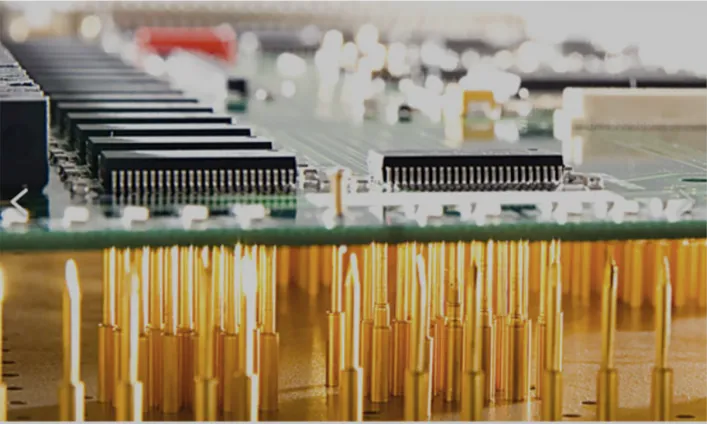
ICT involves applying electrical stimuli through probes to test points on a PCBA, measuring parameters like resistance, capacitance, and diode junctions to detect assembly defects. Bed-of-nails systems use a fixed fixture with spring-loaded probes aligned to a board's test points, enabling high-throughput testing for medium to high volumes. Flying probe alternatives employ movable probes for fixtureless testing, ideal for prototypes or low-volume runs where fixture costs are prohibitive. In the context of miniaturization, ICT ensures micro-components function as specified amid denser layouts and finer features.
The relevance grows as component sizes drop below 0201 metrics, complicating visual and functional inspections. Poor solder joints or misplaced parts can escape optical checks but reveal themselves through ICT's parametric verification. For electrical engineers, ICT provides data-driven insights into assembly quality, reducing field failures and rework costs. Without robust small component testing, high-density boards risk escaping defects that propagate to system-level issues.
Technical Principles Behind SMT ICT Challenges
Miniaturization amplifies SMT ICT challenges through reduced pad sizes and inter-component spacing, often below 0.4 mm. Probes require precise centering to avoid shorts or misses, yet mechanical tolerances limit accuracy to around 0.1 mm in standard setups. PCB warpage from thermal stresses further misaligns test points, demanding compensatory mechanisms in fixtures. Component shielding and high-speed signals introduce guarding needs to isolate measurements accurately.
ICT probe technology relies on Kelvin four-wire connections for low-resistance paths, critical for micro-components where contact resistance skews readings. Fine-pitch arrays like 0.35 mm BGA demand probes with tips under 0.2 mm diameter, pushing material limits for durability. Electrical models simulate board behavior during test development, accounting for parasitics in dense nets. These principles underscore why traditional ICT scales poorly without adaptations.
Adherence to standards like IPC-A-610 for solder joint acceptability guides ICT thresholds, ensuring tests align with production criteria. Engineers must balance test coverage with probe count, as each adds complexity and cost.
Advances in ICT Probe Technology for Small Component Testing
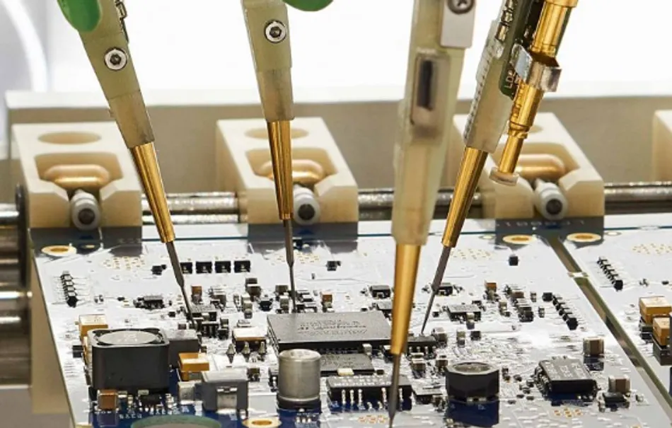
Modern ICT probe technology features micro-probes with diamond or ruby tips for wear resistance and sub-0.1 mm positioning via servo motors and vision alignment. Laser-guided systems achieve repeatability under 50 microns, vital for testing miniaturized PCBs. Hybrid approaches combine bed-of-nails for high-speed nets with flying probes for inaccessible areas. These enable ICT micro components verification even on 0.25 mm pitch devices. Compare these advancements with traditional methods in our ICT Fixture Design Guide: Optimizing PCB Test Coverage.
Boundary scan integration via JTAG/ IEEE 1149.1 complements probing by testing inaccessible nodes digitally. Vectorless tests detect opens without stimuli, reducing fixture complexity. Software advancements allow model-based testing, where golden board data generates limits automatically. Such innovations extend ICT viability into sub-01005 regimes.
Best Practices for Testing Miniaturized PCBs
Design for testability starts with placing dedicated test points on non-critical nets, spaced at 1.91 mm or 2.54 mm grids for fixture compatibility. Use vias as test pads where possible, ensuring annular rings exceed 0.3 mm per IPC guidelines. Limit probe count to under 2000 for cost control, prioritizing high-fault nets. Incorporate guard traces to minimize crosstalk during measurements.
Fixture design demands precise alignment pins and pressure control to counter warpage. Program tests with tolerance bands per component datasheets, verifying against J-STD-001 soldering requirements. Calibrate probes regularly and employ Kelvin sensing for accuracy. Combine ICT with AOI upstream to filter gross defects, optimizing throughput.For complete DFT strategies, see our guide on Design for Testing (DFT) Strategies for IPC Compliant PCBs.
Validate setups on golden boards, iterating to eliminate false calls from probing artifacts. For flying probe, sequence probes to minimize travel time.
Troubleshooting SMT ICT Challenges in Micro-Component Assemblies
Common issues include open circuits from insufficient solder volume on small pads, detectable via high resistance readings. Misaligned probes cause intermittent contacts, addressed by vision verification. Dense ground planes induce capacitive coupling, mitigated by active guarding circuits. Warped boards lift probes, requiring vacuum hold-downs or mechanical compensation.
False positives arise from tolerance drifts in passives; refine limits using statistical analysis. For BGAs, underfill voids evade probes but show as parametric shifts. Systematic debugging involves isolating nets and re-probing suspect areas. Following IPC-6012 performance specs ensures boards meet baseline integrity before ICT.
A typical case involves a high-density IoT module where 01005 capacitors failed continuity tests. Root cause traced to stencil misalignment, corrected by refining print parameters. Such insights highlight ICT's diagnostic power.
Conclusion
ICT remains indispensable for testing miniaturized PCBs despite SMT ICT challenges posed by micro-components. Advances in probe technology and DfT practices enable reliable small component testing, upholding quality in shrinking electronics. Electrical engineers benefit from structured approaches that integrate standards like IPC-A-610 and J-STD-001. Prioritizing testability from design yields higher first-pass rates and robust products. As densities rise, evolving ICT strategies will sustain manufacturing excellence.
FAQs
Q1: What are the main SMT ICT challenges when testing miniaturized PCBs?
A1: SMT ICT challenges stem from fine-pitch components and limited access, such as 0.3 mm spacing that strains probe alignment. Warpage and shielding complicate measurements, while high densities increase crosstalk risks. Best practices include DfT with adequate test points and flying probe systems for flexibility. These ensure accurate verification of ICT micro components without excessive false calls.
Q2: How does ICT probe technology handle small component testing?
A2: ICT probe technology uses micro-tips with vision guidance for sub-0.1 mm precision on tiny pads. Kelvin connections minimize errors in resistance checks for passives. Flying probes adapt to irregular layouts, ideal for prototypes. Combined with guarding, it reliably tests ICT micro components down to 01005 sizes.
Q3: What best practices improve testing miniaturized PCBs with ICT?
A3: Incorporate test points on 2.54 mm grids, use vias for access, and limit probes to essentials. Align fixtures with vision systems and program per component specs. Integrate boundary scan for hidden nodes. These steps address SMT ICT challenges effectively.
Q4: Why is ICT critical for micro-components on high-density boards?
A4: ICT verifies solder integrity and values on micro-components that optical methods miss. It detects opens, shorts, and polarity issues early, per standards like J-STD-001. For miniaturized PCBs, it prevents downstream failures in compact systems.
References
IPC-A-610H — Acceptability of Electronic Assemblies. IPC, 2020
J-STD-001J — Requirements for Soldered Electrical and Electronic Assemblies. IPC, 2024
IPC-6012E — Qualification and Performance Specification for Rigid Printed Boards. IPC, 2017