


PCB Manufacturing
Printed Circuit Boards (PCBs) form the backbone of modern electronics, serving as the essential platform where components connect to create functional devices. In the PCB Manufacturing category, readers gain access to a comprehensive collection of resources designed to demystify the intricate processes involved in producing these critical elements. From initial design considerations to final assembly and testing, this category covers every stage, providing valuable insights for engineers, hobbyists, and industry professionals alike. Understanding PCB manufacturing is crucial for anyone involved in electronics development. This field encompasses a wide range of topics, including material selection, such as FR-4 substrates and advanced laminates, as well as fabrication techniques like etching, drilling, and soldering. Articles here delve into best practices for optimizing layouts to minimize signal interference, ensuring reliability in high-stakes applications. Tutorials guide users through prototyping methods, while in-depth analyses explore emerging trends like flexible PCBs and additive manufacturing, which are revolutionizing industries from consumer gadgets to aerospace systems. The practical value of mastering PCB manufacturing extends to real-world scenarios, where efficient production can reduce costs, enhance performance, and accelerate time-to-market. For instance, insights on multilayer board construction help in designing compact devices for IoT applications, and discussions on quality control standards prevent common pitfalls in mass production. By engaging with the diverse guides and expert perspectives in this category, readers can build a solid foundation in PCB technologies, apply proven strategies to their projects, and stay ahead in an ever-evolving field. Whether troubleshooting assembly issues or exploring sustainable manufacturing practices, the knowledge shared here empowers informed decision-making and innovation in electronics.
Latest Blogs
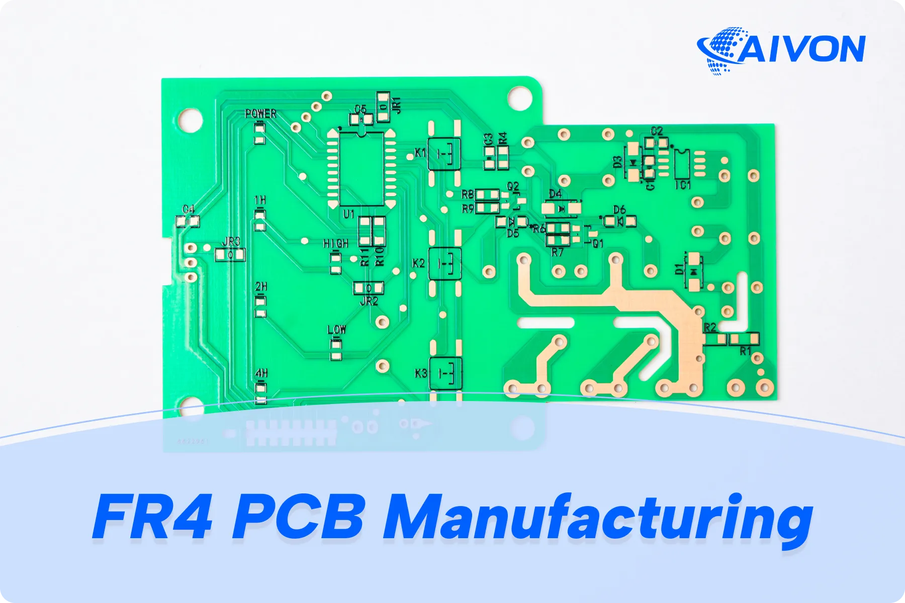
FR4 PCB Manufacturing: Materials, Process, and Fabrication Guide
Learn what FR4 materials are, how FR4 PCBs are made, and how to specify Tg, Td, stackup, and surface finish.
14 Common PCBA Test Methods
Overview of 14 PCB and PCBA test methods to detect defects, guide troubleshooting, and ensure manufacturing quality across assembly inspection and reliability checks.
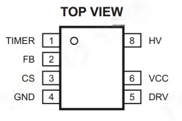
AC-DC Power Conversion: Circuit Methods, HFC0500 Example, and PCB Layout Rules
Learn how AC-DC power supplies convert 220 V AC to DC rails, compare transformer and switching methods, examine an HFC0500 circuit, and apply key PCB layout rules.
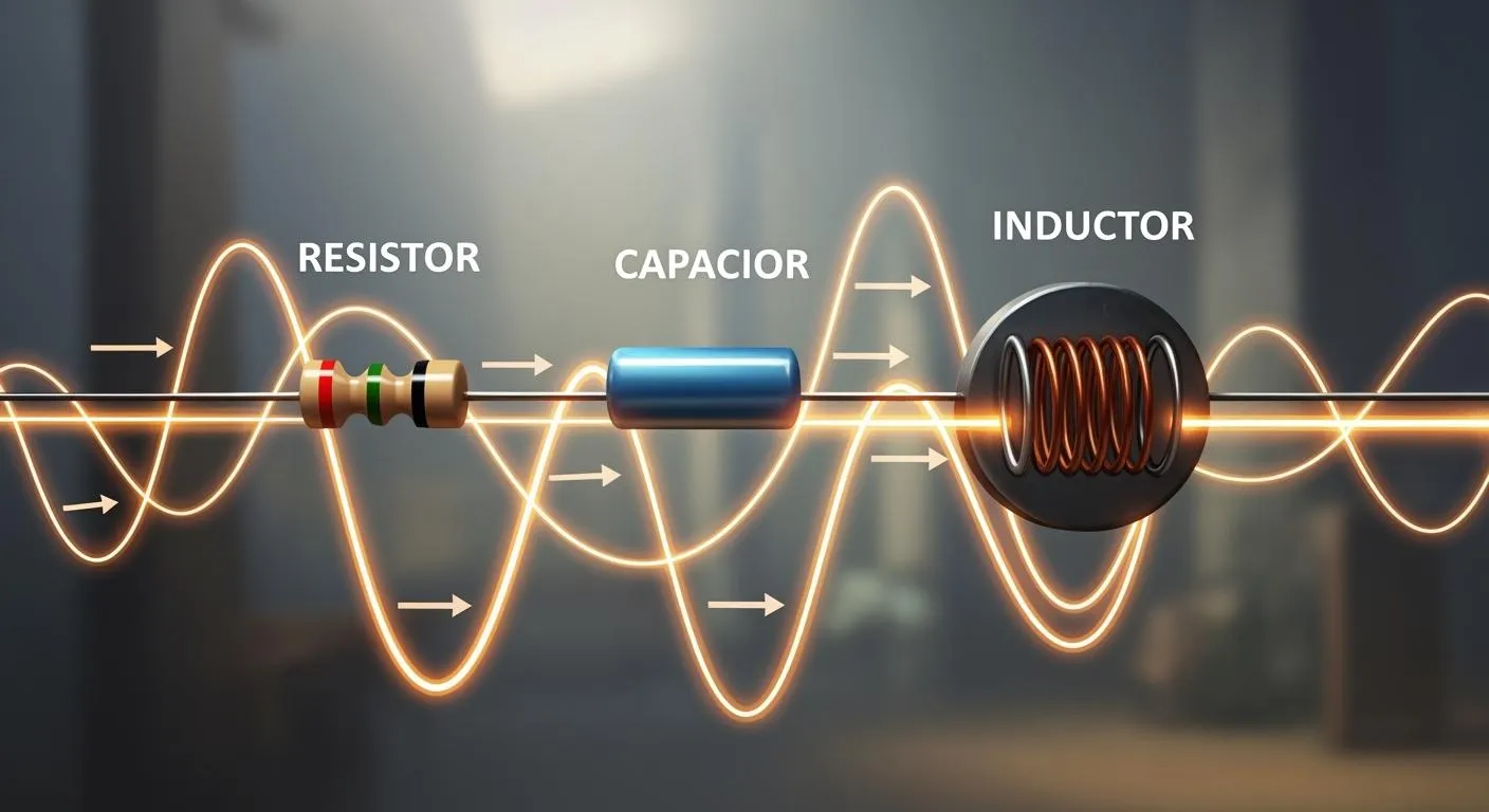
Why Capacitor Voltage and Inductor Current Cannot Change Instantly
Why capacitor voltage and inductor current change continuously: charge and flux cannot jump, energy is conserved, and Faraday's law sets a smooth transition to a new state.

Crystal Oscillator Design Mistakes That Cause Intermittent Startup Failure
Why MCU crystal oscillators fail to start in production: load capacitance and Cs, negative resistance vs ESR, Pierce feedback resistors, layout, drive level, and lot testing.
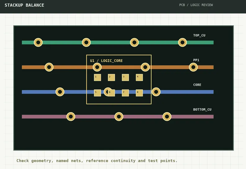
Why a PCB Still Warps When Copper Thickness Is the Same but the Stackup Is Asymmetric
Same layer count and copper thickness do not guarantee a balanced PCB. Check midplane-mirrored materials, dielectric thickness, and zonal copper to reduce bow and twist.
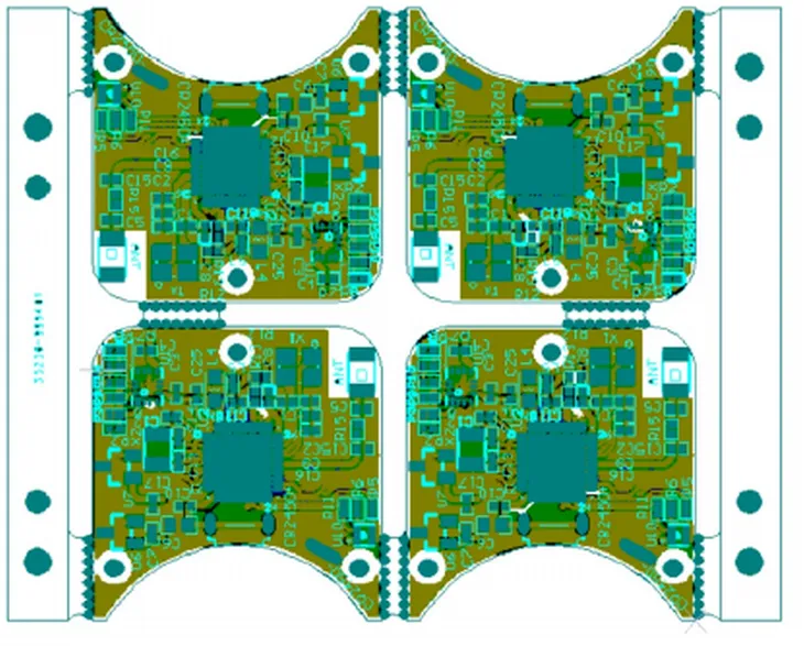
Why a Pick-and-Place Machine Can Still Fail Fiducial Recognition When Three Marks Are Present
Fiducial count is not enough. Contrast, keep-out, three-point span, and panel versus board datums decide whether a pick-and-place machine can lock coordinates.
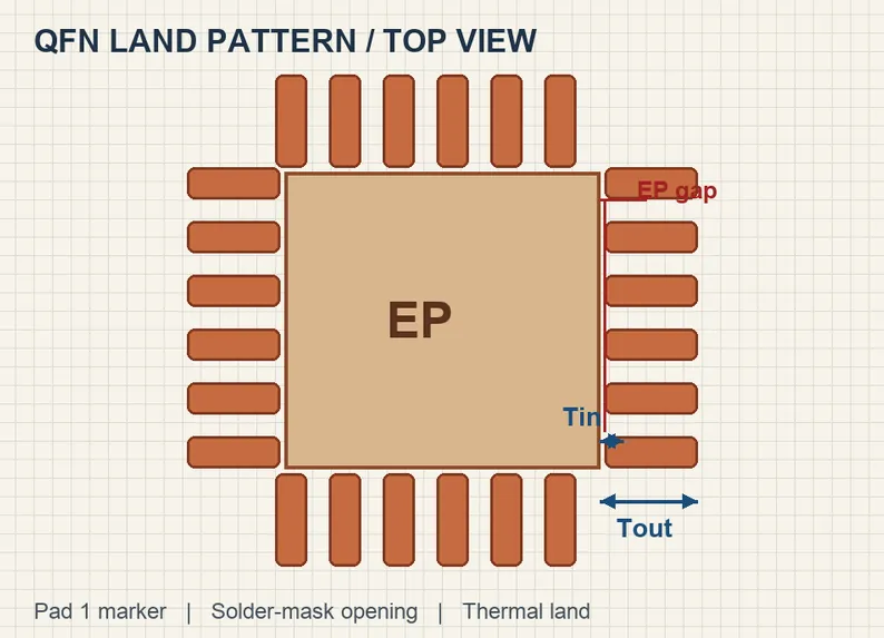
Why Extending QFN Pads Inward Makes Solder Bridging to the Thermal Pad More Likely
Extending QFN pads inward reduces clearance to the thermal pad. Learn why Tin, Tout, solder mask, and stencil design must be reviewed separately to prevent hidden solder bridges.
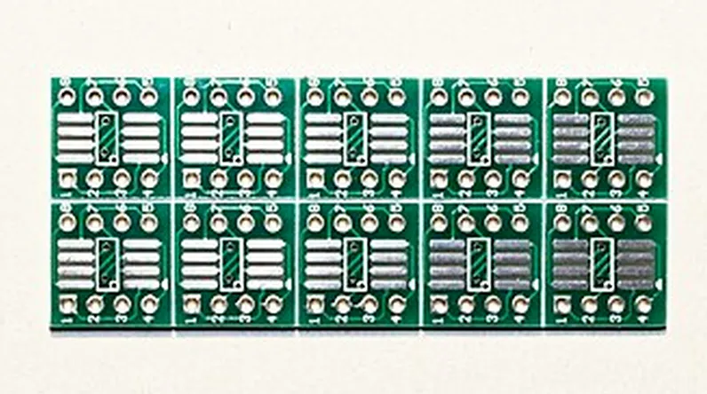
Why Do Copper Traces Near V-CUT Edges Crack During Depaneling?
Why PCB Traces Crack Near V-CUT Edges During Depaneling
HDI PCB Manufacturing Guide: Microvia Technology, Structures and Capabilities
Complete HDI PCB manufacturing guide covering microvia formation, laser drilling, sequential build-up, material selection, quality control, and process parameters that determine density, yield, and reliability.

FR4 PCB Resin Void: Causes and Manufacturing Prevention
Discover FR4 PCB resin void causes in production: resin flow limits, copper structure, and lamination params. Factories reduce resin void in PCB via high-resin prepreg and process control for higher yield.
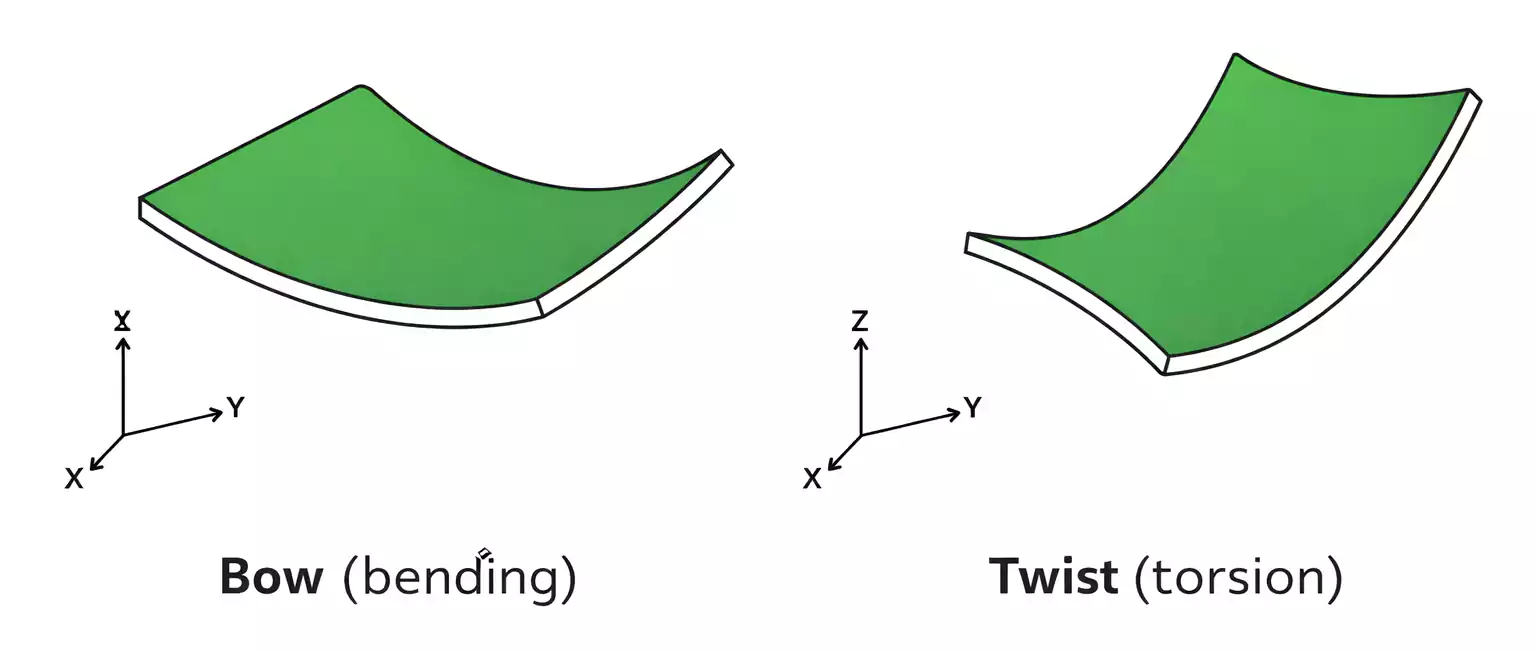
FR4 PCB Warpage and Twist: Manufacturing Causes and Solutions
FR4 PCB warpage and twist arise from copper imbalance, CTE mismatch and thin structures. Factories control them with copper balancing, symmetric stacks, slow cool-down and weighted baking to protect yield and assembly.


