Introduction
Printed circuit board (PCB) rework represents a significant cost in electronics production, often stemming from design oversights that manifest during fabrication or assembly. Implementing a thorough Design for Manufacturability (DFM) review process early in the design cycle enables PCB rework reduction by identifying potential issues before production begins. Electrical engineers focused on PCB design error prevention benefit from this structured approach, as it aligns designs with manufacturing capabilities and improves PCB manufacturability. Factory-driven DFM practices ensure higher yields and shorter lead times, minimizing scrap and delays. This article explores the DFM review process, common pitfalls, and best practices to master it effectively.
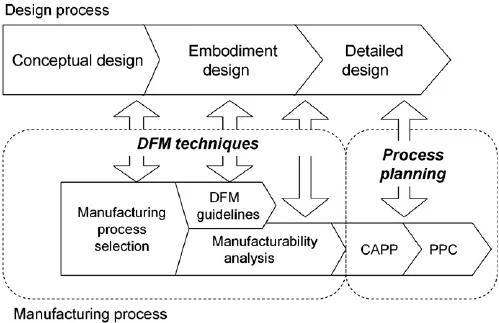
What Is the DFM Review Process and Why Does It Matter?
The DFM review process involves a systematic evaluation of PCB designs against manufacturing constraints, standards, and equipment limitations to ensure reliable production. It typically occurs after schematic completion and initial layout but before Gerber file finalization, allowing iterative improvements. In high-volume manufacturing, poor DFM leads to defects like opens, shorts, or warpage, driving up costs through rework or scrapping entire panels. For electrical engineers, mastering DFM best practices translates to fewer prototypes needed and faster time-to-market. Industry data underscores its value: proactive DFM can cut rework by addressing issues upstream.
From a factory perspective, the review bridges design intent with process realities, such as etching tolerances or plating uniformity. Compliance with standards like IPC-6012 reinforces this by specifying performance criteria for rigid boards. Ultimately, DFM to avoid PCB errors fosters collaboration between design teams and fabricators, enhancing overall product quality.
Common Causes of PCB Rework: Key Design Pitfalls
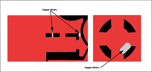
PCB rework often traces back to fabrication challenges, where design features exceed standard process windows. Acid traps, formed by acute angles in copper traces, trap etchant and cause undercuts or opens during inner layer etching. Slivers—tiny copper fragments from overlapping geometries—similarly disrupt plating and inspection. These issues highlight the need for smooth, manufacturable geometries in layouts.
Assembly-related rework arises from inadequate land patterns or spacing. Tombstoning occurs when surface-mount components lift due to uneven reflow heating, often from asymmetric pad sizes or poor thermal reliefs. Solder bridging between fine-pitch parts results from insufficient solder mask dams or paste mask misalignment. Factory insights reveal that via-in-pad designs without proper fill specifications lead to solder wicking, complicating assembly.
Warpage, a frequent culprit in multilayer boards, stems from asymmetric stackups where copper distribution imbalances CTE stresses during lamination or reflow. Non-uniform panelization, lacking fiducials or tooling holes, misaligns during automated handling, causing registration errors. These defects not only demand rework but also lower yields, emphasizing PCB design error prevention through balanced designs.
Mechanical tolerances play a role too. Oversized holes relative to pads reduce annular rings below acceptable limits, risking drill breakout or plating voids. Silkscreen overlapping solder masks obscures markings, complicating inspection per IPC-A-600 criteria for board acceptability. Addressing these in DFM reviews prevents downstream quality escapes.
Mastering the DFM Review: Structured Best Practices
A factory-aligned DFM review starts with layer stackup optimization to improve PCB manufacturability. Symmetric constructions, with balanced core and prepreg thicknesses, mitigate warpage by equalizing thermal expansion. Engineers should verify copper weight distribution across layers to avoid bow and twist exceeding standard allowances. Core-to-core alignment and sequential lamination for high-layer counts further enhance flatness.
Trace and spacing rules form the backbone of routing DFM best practices. Minimum widths and clearances must account for etch factor, ensuring signals maintain integrity without opens. Teardrops at via-to-trace junctions prevent drill smear and cracking under thermal cycling. Curved corners over 45-degree angles reduce stress concentrations and etching inconsistencies.
Pads and vias demand precise sizing. Annular rings around holes should provide sufficient landing for plating, with via tents or plugs preventing solder exposure during assembly. Filled or tented vias in high-density areas avoid chemical residue buildup. Factory processes favor standard drill sizes to minimize tool wear and maintain hole quality.
Solder mask and silkscreen layers require expansion rules to clear pads adequately, avoiding bridging while maintaining coverage. Mask registration tolerances ensure no exposure on fine features. Silkscreen legends positioned away from edges and fiducials aid automated optical inspection.
Panelization best practices include multiple fiducials—3mm diameter, non-plated—for alignment, plus tooling holes at corners. V-scoring or tab routing must respect board thickness to prevent chipping. Depanelization simulations confirm stress-free separation.
Material selection ties into DFM, matching CTE between components and substrate to reduce assembly stresses. High-Tg laminates support lead-free reflow per J-STD guidelines. Documentation completeness, including fab and drill drawings, closes the review loop.
- Stackup: Symmetry, copper balance, sequential lamination
- Routing: Trace width/spacing, teardrops, no acute angles
- Pads/Vias: Annular ring, tenting/fill, standard drill sizes
- Mask/Screen: Expansion, registration, clearances
- Panelization: Fiducials, tooling holes, depanel method
Troubleshooting Real-World DFM Scenarios
Consider a multilayer design exhibiting post-reflow warpage, traced to unbalanced copper planes. A DFM review revealed heavier outer layers; redistributing ground pours and adding dummy fills resolved it without respin. In another case, fine-pitch BGA assembly failures from via breakout prompted annular ring verification against IPC-6012, leading to larger antipads.
These scenarios illustrate iterative DFM: simulate stackup, run DRCs, and solicit fabricator feedback. Early detection via review checklists prevents escalation.
Conclusion
Mastering the DFM review process is essential for PCB rework reduction and sustained manufacturability gains. By addressing stackup, routing, and documentation systematically, electrical engineers prevent common errors proactively. Adhering to standards like IPC-A-600 ensures acceptability from fab to assembly. Implement these DFM best practices to streamline production, boost yields, and deliver reliable boards.
FAQs
Q1: What is DFM in the context of PCB design error prevention?
A1: DFM, or Design for Manufacturability, is a review process that evaluates PCB layouts against fabrication and assembly constraints. It identifies issues like inadequate clearances or asymmetric stackups early, preventing defects that cause rework. Factory-aligned checks improve PCB manufacturability by aligning designs with process capabilities, reducing scrap rates.
Q2: How can engineers achieve PCB rework reduction through DFM best practices?
A2: Start with symmetric stackups and standard trace rules to avoid warpage and etching failures. Include fiducials and proper panelization for alignment. Verify annular rings and mask expansions per industry guidelines. This systematic approach catches errors pre-production, minimizing assembly issues like bridging.
Q3: Why is layer stackup critical for improving PCB manufacturability?
A3: Unbalanced stackups induce thermal stresses, leading to warpage during lamination or reflow. Symmetric designs with balanced copper distribution maintain flatness within tolerances. DFM reviews simulate these effects, ensuring compliance and high yields in multilayer boards.
Q4: What role do standards play in DFM to avoid PCB errors?
A4: Standards like IPC-6012 define performance specs for boards, guiding trace sizing and hole quality. IPC-A-600 sets acceptability criteria for visual and mechanical features. Integrating them into reviews standardizes practices across factories, preventing variability-induced rework.
References
IPC-6012F — Qualification and Performance Specification for Rigid Printed Boards. IPC, 2023
IPC-A-600K — Acceptability of Printed Boards. IPC, 2020
IPC-2221B — Generic Standard on Printed Board Design. IPC, 2003
J-STD-001GS — Requirements for Soldered Electrical and Electronic Assemblies. IPC, 2020


