Introduction
Transitioning from PCB prototyping to full-scale production presents unique challenges for electrical engineers. While prototypes validate circuit performance under controlled conditions, production demands robustness against manufacturing variations. Mastering manufacturability checks ensures designs translate seamlessly into high-yield runs. These checks encompass design for manufacturing (DFM) best practices that address fabrication tolerances, assembly compatibility, and material behaviors. By integrating DFM early, teams avoid costly respins and delays. This article explores structured approaches to PCB prototyping and scaling to production, emphasizing factory-driven insights aligned with industry standards.
What Is PCB Manufacturability and Why It Matters for Scaling to Production
PCB manufacturability refers to the ease with which a design can be fabricated and assembled at scale without compromising quality or incurring excessive costs. In prototyping, engineers often prioritize speed, using relaxed tolerances that work for low volumes but fail in production. Scaling to production amplifies issues like warpage, delamination, or solder defects due to process variations across panels and lots. Effective manufacturability checks mitigate these risks, ensuring consistency from first article to millions of units. Poor DFM leads to yield losses exceeding 20 percent in early runs, inflating costs and timelines. Ultimately, strong manufacturability supports reliable performance in end applications, from consumer electronics to aerospace systems.
Adhering to standards like IPC-2221C provides a baseline for design rules that factories can consistently meet. This standard outlines generic requirements for printed board design, including spacing, vias, and thermal management. Why does this matter? Production environments impose stricter controls on parameters like drill accuracy and plating uniformity, which prototypes may overlook. Engineers who embed DFM best practices reduce iteration cycles, fostering smoother PCB manufacturer communication. The result is accelerated time-to-market and enhanced product reliability.
Key Technical Principles of PCB Manufacturability
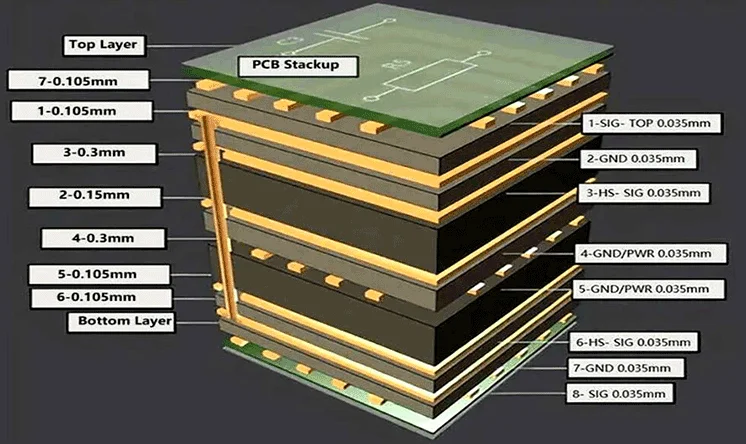
Understanding the core mechanisms behind PCB fabrication reveals why certain design choices impact scalability. Layer stackup symmetry prevents warpage during lamination and reflow, as uneven copper distribution induces thermal stresses. Copper balance across layers maintains planarity, critical for high-density interconnects. Vias demand precise sizing and plating to avoid stub effects or reliability failures under thermal cycling. Clearances and spacings must accommodate etching tolerances, preventing shorts or opens in volume production.
Material selection influences these principles profoundly. Dielectrics with controlled coefficients of thermal expansion minimize mechanical stresses at copper interfaces. Aspect ratios for vias and holes limit drill wander and plating voids, principles embedded in qualification specs like IPC-6012F. This standard specifies performance requirements for rigid printed boards, including electrical and mechanical tests. Surface finishes affect solderability and shelf life, requiring compatibility with assembly processes. Engineers must model these interactions early to predict production outcomes.
Routing geometry further dictates manufacturability. Acute angles in traces promote etching undercuts, while teardrops at pads distribute stresses and improve yield. Panelization introduces edge effects, necessitating breakaway tabs and fiducials for accurate registration. These elements ensure robotic handling and alignment during scaling to production. Thermal management principles, such as via tents and plane cutouts, prevent issues like solder wicking into vias during reflow.
DFM Best Practices: Essential Checks from Design to Fabrication
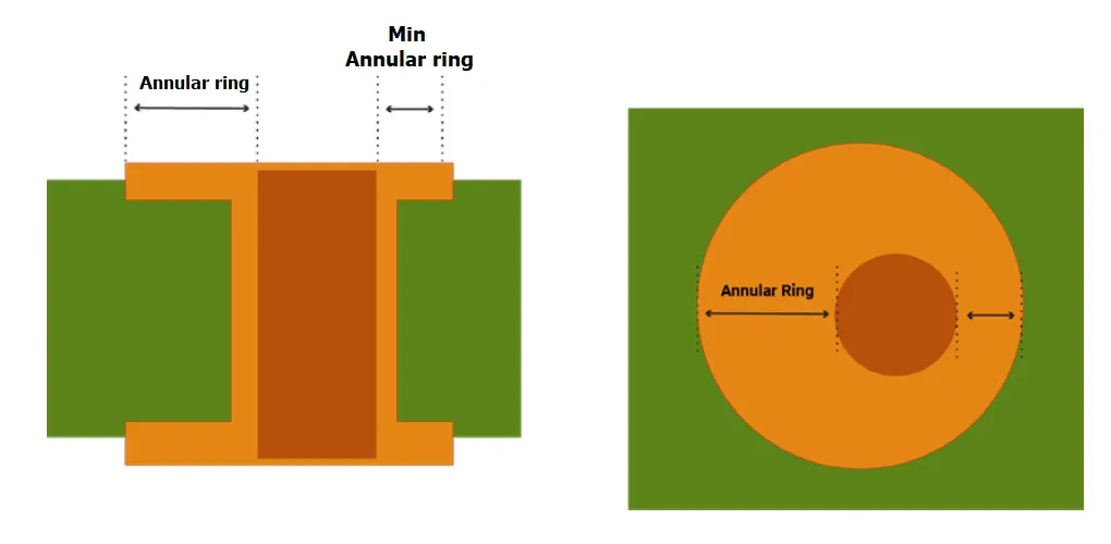
Implementing DFM best practices starts with a comprehensive checklist during PCB prototyping. Verify trace widths and spacings against class levels defined in standards, adjusting for production etch factors. Annular rings around pads and vias should provide margins for misalignment, typically larger for inner layers. Use standard drill sizes to leverage factory tooling, reducing setup times and costs. Copper pours demand balanced fills to avoid plating anomalies.
For multilayer boards, prioritize symmetric stackups and controlled impedance where signal integrity matters. Simulate warpage using finite element analysis if high copper asymmetry exists. Incorporate test points and fiducials in corners for probing and alignment. IPC-A-600M guides acceptability criteria, distinguishing target conditions from acceptable ones post-fabrication. This standard details visual and dimensional inspections for printed boards.
Assembly-focused DFM includes land patterns optimized for component types, avoiding tombstoning or bridging. Stencil apertures require adjustments for fine-pitch parts, ensuring uniform paste deposition. Panel design supports multiple-up arrays with v-scoring or tab routing for depanelization. During scaling to production, validate first articles against these checks before full release.
Common Pitfalls in PCB Prototyping and Scaling to Production
Engineers often encounter pitfalls when rushing prototypes without production foresight. Oversized panels exceed handling limits, causing registration errors. Non-standard hole sizes force custom drills, escalating costs. Ignoring copper balance leads to bow and twist beyond tolerances, complicating assembly.
Another frequent issue is inadequate via protection, resulting in solder fill during reflow. Prototype success with quick-turn materials may not scale, as production uses higher-Tg laminates for stability. Poor silkscreen registration obscures markings, violating readability requirements. Effective troubleshooting involves iterative DFM reviews, catching these before quoting.
Communication gaps exacerbate pitfalls. Assumptions about capabilities lead to mismatched expectations. Sharing stackup details and impedance specs upfront aligns processes.
Optimizing PCB Manufacturer Communication for Smooth Transitions
Clear PCB manufacturer communication is pivotal for manufacturability success. Provide complete gerber, drill, and fab drawings with notes on class level and special processes. Discuss stackup early to confirm material availability and press cycles. Request DFM feedback during quoting to preempt issues.
Specify inspection criteria per IPC standards, including AQL levels for production. For scaling to production, qualify processes with coupon tests for plating and etch. Regular reviews of first articles refine future interactions. This collaborative approach minimizes surprises and optimizes yields.
Conclusion
Mastering PCB manufacturability checks transforms prototypes into production-ready designs. By embedding DFM best practices, engineers address technical principles like stackup symmetry and routing integrity. Standards such as IPC-2221C, IPC-6012F, and IPC-A-600M provide factory-aligned guidance. Proactive PCB manufacturer communication ensures seamless scaling to production. These strategies yield higher reliability, lower costs, and faster market entry. Prioritize manufacturability from day one for enduring success.
FAQs
Q1: What are the core DFM best practices for PCB prototyping?
A1: DFM best practices include verifying trace spacings, annular rings, and via sizes against standards like IPC-2221C. Balance copper distribution to prevent warpage and use standard drill diameters for efficiency. Incorporate fiducials and test points for assembly alignment. These steps ensure designs scale reliably to production without redesigns.
Q2: How does design for manufacturing impact scaling to production?
A2: Design for manufacturing optimizes layouts for fabrication tolerances, reducing defects in high-volume runs. It addresses issues like etch undercuts and plating uniformity early. Factories achieve higher yields when prototypes follow DFM, minimizing respins. Effective practices cut costs by 15-30 percent through fewer iterations.
Q3: Why is PCB manufacturer communication essential during manufacturability checks?
A3: PCB manufacturer communication clarifies capabilities for stackups, finishes, and tolerances. Sharing detailed drawings elicits targeted DFM feedback, avoiding mismatches. It aligns expectations on class levels and inspections per IPC-A-600M. Strong dialogue accelerates transitions from prototyping to production.
Q4: What role do industry standards play in PCB manufacturability?
A4: Standards like IPC-6012F define performance specs for rigid boards, guiding qualification tests. They establish consistent criteria for acceptability and design rules. Factories rely on them for process controls, ensuring scalability. Engineers referencing these minimize risks in production.
References
IPC-2221C — Generic Standard on Printed Board Design. IPC, 2023
IPC-6012F — Qualification and Performance Specification for Rigid Printed Boards. IPC, 2023
IPC-A-600M — Acceptability of Printed Boards. IPC, 2025


