Introduction
In electronics manufacturing, the assembly process often determines the success of a product, especially for printed circuit boards (PCBs) packed with surface-mount devices (SMDs) and through-hole components. Design for Assembly (DFA) emerges as a critical methodology that streamlines this phase by optimizing designs from the outset. Electric engineers benefit greatly from DFA for electronics, as it minimizes errors during pick-and-place, soldering, and inspection. This guide explores DFA principles, benefits, and practical steps tailored for high-volume production. Whether troubleshooting yield issues or planning new layouts, mastering DFA reduces rework and accelerates time-to-market. By focusing on assembly-friendly features, engineers can achieve reliable outcomes without compromising functionality.
What Is Design for Assembly (DFA) in Electronics Manufacturing?
Design for Assembly (DFA) refers to a systematic approach in product design that simplifies the assembly process while maintaining performance requirements. In electronics, DFA targets PCB layouts, component selection, and fabrication to facilitate automated and manual assembly. Core goals include reducing part count, standardizing orientations, and ensuring accessibility for tools like pick-and-place machines and reflow ovens. Unlike general design rules, DFA specifically addresses manufacturing constraints, such as stencil printing alignment and solder joint formation. Engineers apply DFA early in the design cycle to avoid costly iterations later. This proactive strategy aligns with industry needs for higher throughput and fewer defects.
DFA principles draw from broader design for manufacturability concepts but emphasize assembly-specific challenges. For instance, uniform component spacing prevents collisions during robotic placement. Fiducial marks serve as reference points for machine vision systems, ensuring precise registration. Polarity indicators on components eliminate orientation mistakes that lead to functional failures. By integrating these elements, DFA transforms complex boards into efficient assemblies. Electric engineers often use DFA checklists during reviews to catch potential issues before prototyping.
Why DFA Matters: DFA Benefits in Manufacturing
DFA benefits in manufacturing extend beyond immediate cost savings to long-term reliability and scalability. First, it shortens assembly cycle times by enabling faster machine throughput and fewer handling steps. Reduced part variety lowers inventory needs and simplifies supply chains, critical for just-in-time production. Defect rates drop significantly because designs avoid common pitfalls like shadowing during reflow or mechanical stress on joints. In high-mix, low-volume runs, DFA supports flexibility without sacrificing quality.
From a troubleshooting perspective, DFA minimizes root causes of failures such as tombstoning or bridging in solder joints. Optimized pad geometries promote even solder flow, adhering to soldering standards like J-STD-001. Yield improvements translate to higher first-pass success, reducing scrap and rework labor. Scalability becomes evident in volume ramps, where DFA-optimized boards handle increased speeds without proportional error growth. Engineers report smoother transitions from prototype to production, with fewer engineering change orders. Ultimately, DFA aligns design intent with factory realities, fostering collaboration between teams.
Key Principles of DFA for Electronics
The foundation of DFA for electronics lies in minimizing complexity while maximizing automation compatibility. Principle one: reduce component count by multifunction integration, such as combining resistors into networks. This cuts placement operations and inspection points. Standardize package types and sizes across the board to streamline feeder setups in assembly lines. Orient all polarized components consistently, typically with cathode or pin 1 facing the same direction. These steps prevent programming errors in machine software.
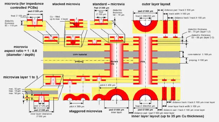
Accessibility ranks high in DFA principles. Ensure no tall components block adjacent low-profile ones during placement sequences. Maintain adequate spacing between parts, typically following land pattern guidelines from IPC-2221. Provide three fiducials per panel, asymmetrically placed for unambiguous detection. Avoid placing fine-pitch parts near board edges to prevent handling damage. Troubleshooting tip: simulate assembly paths virtually to identify interference early.
Soldering compatibility forms another pillar. Design pad sizes and shapes to match component leads precisely, promoting self-alignment during reflow. Incorporate via-in-pad restrictions to avoid solder wicking that causes opens. Use no-clean fluxes compatible with assembly environments to simplify post-process cleaning. Thermal balance prevents warping, ensuring uniform heating. Engineers troubleshoot by analyzing reflow profiles against component tolerances.

DFA Implementation Guide: Step-by-Step Approach
Implementing DFA starts with a design review checklist tailored to electronics assembly. Begin by auditing the bill of materials (BOM) for part standardization and availability. Eliminate unnecessary components through circuit optimization, such as passive networks. Group similar packages by function zones to optimize travel paths for placement heads. Define panelization rules, like V-scoring or tab routing, for stable handling.
Next, focus on layout strategies. Place high-precision parts centrally, away from edges prone to flexing. Ensure stencil apertures match pad dimensions with appropriate release areas to control solder paste volume. Incorporate test points accessible post-assembly without special fixtures. Simulate thermal profiles to verify no hot spots cause delamination. For mixed-technology boards, sequence through-hole after SMT to avoid contamination.
Validation involves prototyping and analysis. Run design rule checks (DRC) against assembly tolerances. Conduct trial runs to measure placement accuracy and first-pass yield. Adjust based on data, such as increasing keep-out zones for adhesives. Document changes in a DFA report for future projects. This iterative process ensures robust implementation.
DFA Best Practices in Electronics Manufacturing
DFA best practices electronics emphasize proactive measures grounded in real-world assembly dynamics. Standardize component orientation to a single direction, reducing setup time by up to programming complexities. Use 0603 or larger SMDs where possible for better handling by nozzles, reserving 01005 for critical needs. Implement edge clearance of at least 5 mm for grippers and avoid vias under components to prevent solder entrapment.
Panel design merits special attention. Array boards with consistent spacing, including tooling holes for fixtures. Place fiducials outside the product area, at least 3 mm from edges. For wave soldering in through-hole sections, orient leads to minimize bridging risks. Adhere to cleanliness standards by specifying no-flux zones near connectors.
Troubleshooting common issues enhances best practices. For tombstoning, balance pad sizes with larger lands on the component side. Bridging responds to reduced paste volumes via trapezoidal stencils. Warpage control involves symmetric copper distribution and bake-out before assembly. Reference IPC-A-610 criteria during inspections to classify defects objectively.
DFA Examples: Real-World Applications and Lessons
Consider a multilayer PCB for consumer devices with dense BGA placement. Pre-DFA, misalignment caused 15% rework due to insufficient fiducials and irregular spacing. Post-DFA redesign added dedicated fiducials, zoned layouts, and via plugging under balls. Assembly yield jumped, with placement accuracy within 50 microns. Lesson: early fiducial integration pays dividends in high-density boards.
In automotive electronics, a power module faced reflow failures from thermal mismatch. DFA application standardized QFN packages, added thermal vias with filled plating, and balanced copper pours. Solder joint integrity improved per J-STD-001, eliminating voids. Troubleshooting revealed initial pad etch issues; resizing per land pattern standards resolved them. This example underscores thermal DFA's role in reliability.
Another case involved IoT sensors with mixed SMD and THT. Original design clustered THT near SMT, complicating sequencing. DFA separated zones, used wave-compatible pins, and added masking for selective soldering. Throughput increased without yield loss. Key takeaway: zoning prevents process conflicts.
Common Pitfalls and Troubleshooting in DFA
Even with DFA, pitfalls arise from overlooked details. Insufficient edge support leads to panel flex during transport, misaligning fiducials. Solution: reinforce with breakaway tabs and specify material stiffness. Polarity marking omissions cause batch failures; always mandate silkscreen legends matching datasheets.
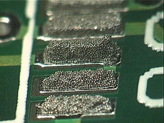
Solder defects like head-in-pillow stem from paste misalignment. Troubleshoot by verifying stencil thickness and snap-off distance. Component offset during reflow signals poor self-centering; enlarge toe pads slightly. For fine-pitch QFNs, exposed pads demand precise via fencing to escape gases. Regular SPI and AOI feedback loops refine practices.
Handling mixed assemblies challenges DFA. THT clips can shadow SMDs; sequence carefully and use pallets. Moisture sensitivity amplifies issues; bake components pre-assembly. Systematic root-cause analysis, tied to standards, resolves these efficiently.
Conclusion
Design for Assembly (DFA) stands as an indispensable tool for electric engineers in electronics manufacturing. By embedding DFA principles early, teams unlock benefits like faster cycles, lower defects, and scalable production. The DFA implementation guide and best practices outlined here provide actionable paths forward. DFA examples illustrate transformative impacts on real projects. Prioritize troubleshooting integration for sustained gains. Embrace DFA to bridge design and assembly seamlessly, ensuring robust, efficient electronics.
FAQs
Q1: What are the primary DFA benefits in manufacturing for electronics?
A1: DFA benefits in manufacturing include reduced assembly time through standardized parts and optimized layouts, lower defect rates from better solderability, and cost savings via minimized rework. It enhances yield by preventing issues like misalignment or bridging, supports automation, and improves scalability for volume production. Electric engineers see faster prototyping cycles and reliable field performance. Overall, DFA aligns design with factory capabilities effectively.
Q2: How can engineers follow a DFA implementation guide?
A2: Start the DFA implementation guide with BOM review for part standardization, then layout for accessibility and fiducials. Simulate placement and reflow, prototype, and iterate based on yield data. Incorporate zoning for mixed tech and edge supports. Validate against soldering standards. This step-by-step approach minimizes risks and accelerates production readiness.
Q3: What DFA best practices electronics should be prioritized?
A3: Key DFA best practices electronics involve uniform component orientation, adequate spacing, precise fiducials, and pad geometries for self-alignment. Panelize with tooling holes, control stencil apertures, and balance thermals. Avoid vias under parts and mandate clear markings. Regular AOI/SPI troubleshooting refines these for high yields.
Q4: Can you provide DFA examples from PCB assembly?
A4: DFA examples include redesigning dense BGA boards with added fiducials for alignment, improving yield dramatically. Power modules benefit from thermal vias and copper balancing to eliminate voids. IoT boards separate SMT/THT zones to avoid shadowing. These cases show DFA reducing rework through targeted optimizations.
References
IPC-2221G — Generic Standard on Printed Board Design. IPC, 2012
IPC-A-610H — Acceptability of Electronic Assemblies. IPC, 2012
IPC J-STD-001J — Requirements for Soldered Electrical and Electronic Assemblies. IPC, 2024