Introduction
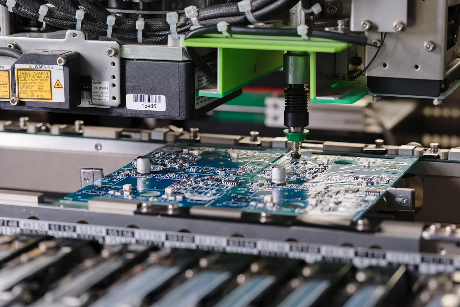
In the fast-paced world of PCB assembly, design flaws can lead to costly rework, delays, and yield losses that frustrate electric engineers and production teams alike. Design for Assembly (DFA) integrates assembly considerations early in the PCB design phase to ensure smooth transitions from layout to fabrication and population. This DFA checklist PCB approach minimizes errors during surface-mount technology (SMT) and through-hole technology (THT) processes, optimizing for automated pick-and-place machines and reflow soldering. By following a structured DFA steps PCB assembly guide, engineers can reduce assembly time, lower defect rates, and improve overall reliability. This article outlines 10 practical steps tailored for electric engineers, drawing on proven troubleshooting strategies to streamline your workflow. Whether dealing with high-density SMT boards or mixed THT assemblies, these guidelines provide actionable insights to enhance manufacturability.
What Is Design for Assembly (DFA) and Why It Matters for PCB
Design for Assembly refers to the practice of optimizing PCB layouts specifically for efficient assembly processes, focusing on reducing complexity and potential failure points. In PCB contexts, DFA bridges design intent with manufacturing realities, addressing challenges like component misalignment, solder joint defects, and handling issues. For electric engineers, it matters because poor DFA leads to common troubleshooting headaches, such as tombstoning in SMT reflow or bridging in THT wave soldering. Industry data shows that effective DFA can cut assembly costs by up to 30% through fewer parts and standardized processes. It aligns with standards like IPC-A-610 for acceptability criteria, ensuring boards meet performance without excessive post-assembly fixes. Ultimately, a solid PCB design for assembly guide prevents downstream issues, speeding time-to-market for prototypes and production runs.
DFA principles emphasize simplicity: minimize part count, standardize footprints, and ensure accessibility for tools like automated optical inspection (AOI). In SMT-dominant designs, DFA prioritizes fiducial accuracy for machine vision; in THT, it focuses on hole-to-lead tolerances to avoid stress during insertion. Neglecting DFA often results in panelization failures or thermal mismatches that warp boards during reflow. Engineers benefit from DFA by gaining predictable yields, easier debugging, and scalability for high-volume assembly. This checklist adapts these concepts into targeted steps, helping you avoid pitfalls proactively.
The 10-Step DFA Checklist for PCB Assembly
Step 1: Verify Footprint Accuracy Against Component Datasheets
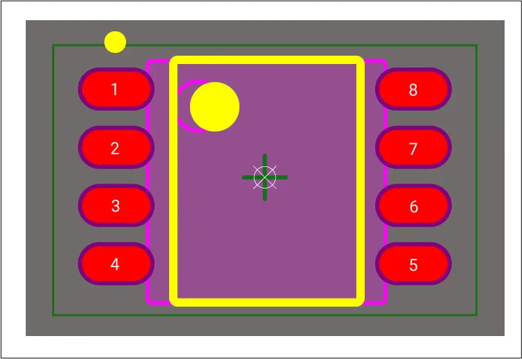
Start your DFA checklist PCB by confirming that all footprints match the latest component datasheets precisely, including pad dimensions, shapes, and tolerances. Misaligned footprints cause placement errors in SMT pick-and-place operations or poor solder wetting in THT insertions, leading to open joints or shorts. Use IPC-7351 land pattern standards to select density levels (e.g., most or nominal) that balance assembly ease with space constraints. For polarized parts like diodes or capacitors, clearly mark pin 1 or polarity indicators in the footprint and silkscreen. Cross-check courtyard keepouts to prevent adjacent component interference during reflow. This step alone resolves many early assembly rejects, ensuring reliable mechanical and electrical connections.
Step 2: Incorporate Fiducial Marks for Precise Alignment
Fiducials are essential reference points for machine alignment in SMT assembly, so place at least three global fiducials at board corners and local ones near dense component groups. Design them as 1 mm diameter, non-plated copper pads without solder mask, with 0.1 mm clearance to the board edge and other features. In panelized arrays, ensure fiducials are consistent across all boards to avoid stencil misalignment during solder paste printing. For THT-heavy boards, fiducials aid selective soldering setup. Troubleshoot common issues by verifying fiducial flatness and avoiding placement under components or traces. Proper fiducials reduce placement offsets to under 0.05 mm, streamlining DFA for SMT assembly.
Step 3: Optimize the Bill of Materials (BOM) for Standardization and Minimization
Review your BOM to minimize unique part counts by selecting standard packages like 0805 resistors or SOIC ICs, which suit automated handling and reduce kitting errors. Eliminate duplicates, verify manufacturer part numbers (MPNs) for availability, and note alternatives for long-lead items. Prioritize lead-free, reflow-compatible parts to avoid mixed soldering processes in hybrid SMT/THT designs. This DFA steps PCB assembly practice cuts inventory costs and assembly steps, as fewer variants mean simpler programming for pick-and-place. Flag odd-form components requiring manual intervention early. A clean BOM prevents procurement delays and supports smooth transitions to assembly.
Step 4: Strategically Group and Orient Components
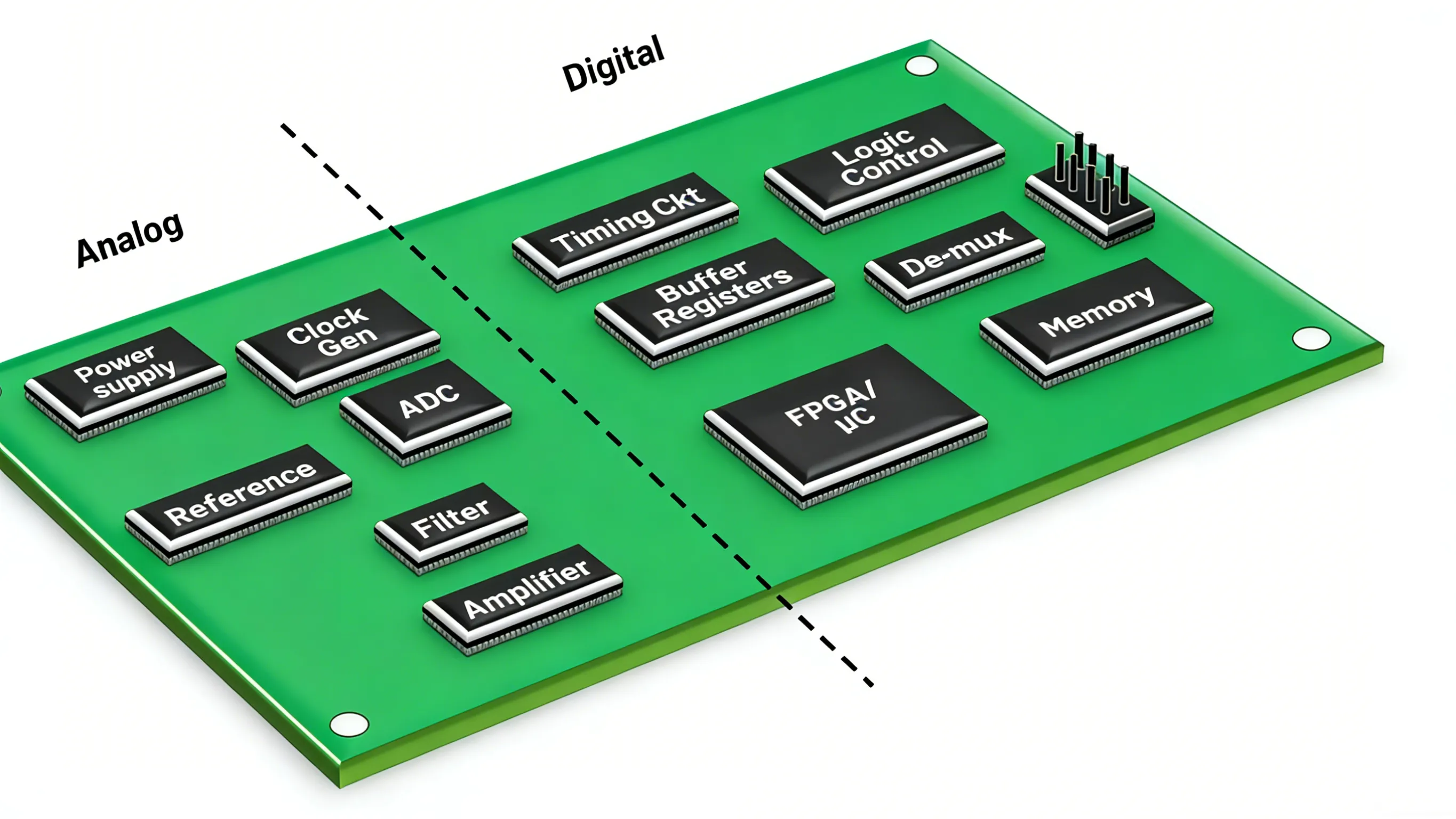
Group components by process type—SMT first, then THT—to enable efficient single-pass reflow followed by wave or selective soldering. Orient polarized parts consistently (e.g., all capacitors with positive lead on the same side) and separate analog from digital sections to minimize noise coupling during assembly testing. Place tall components away from board edges to prevent handling damage, and cluster high-heat parts near edges for fixture clearance. In troubleshooting, uneven orientations cause reflow defects like tombstoning due to asymmetric heating. This layout optimizes machine throughput and eases visual inspection. Balanced placement also aids thermal uniformity, critical for dense boards.
Step 5: Ensure Adequate Clearances and Spacings
Maintain minimum clearances: 0.127 mm between SMT pads, 0.2 mm part-to-part for passives, and 0.2 mm to board edges for depanelization. For THT, ensure 0.2 mm from leads to nearby SMT pads to avoid solder wicking. Component-to-via spacing prevents bridging, while part-to-hole wall distances of at least 0.2 mm accommodate drill tolerances. Troubleshoot overcrowding by simulating solder paste deposition; tight spaces increase bridging risks in reflow. These DFA for SMT assembly rules reduce shorts and improve AOI detection. Consistent spacings also facilitate probe access during in-circuit testing.
Step 6: Design Solder Mask and Paste Layers Precisely
Align solder mask openings 1:1 with pads, maintaining 0.1 mm dams between pads to prevent bridging without restricting solder flow. For exposed pads in QFNs or thermal reliefs, expand mask clearances appropriately. Paste mask reduction (e.g., 0.1 mm smaller than pads) controls volume for consistent reflow joints. In THT, mask vias to avoid solder fill issues. Common troubleshooting: excessive mask encroachment causes weak joints; verify layers in Gerber viewers. This step ensures reliable DFA for THT assembly by minimizing voids and balls.
Step 7: Apply Clear Silkscreen Markings and Reference Designators
Use 0.1 mm minimum line width for silkscreen text, with 0.6 mm height for legibility under AOI, avoiding overlaps with pads or masks. Place reference designators adjacent to components without obscuring polarity marks. Standardize symbols like bar over pin 1 for ICs or '+' for capacitors. For troubleshooting, faint or misaligned silk leads to placement errors. White ink provides best contrast on most finishes. These details speed manual verification and reduce operator errors in mixed assemblies.
Step 8: Integrate Accessible Test Points
Position test points on non-plated pads near critical nets, with 1.5 mm minimum spacing from component leads for probe clearance. For BGAs, avoid under-component points; use edge-accessible vias instead. In THT areas, elongate pads for bed-of-nails fixturing. Formula for probe distance: at least 0.29 times component height plus 0.7 mm. This facilitates functional circuit testing (FCT) without board stress. Troubleshoot by ensuring points survive reflow without lifting.
Step 9: Plan Panelization for Efficient Depaneling
Array boards with 5 mm v-groove spacing, including fiducials and tooling holes (3.2 mm diameter) at corners. Use tab routing over v-scoring near components to prevent chipping. Orient all units identically for consistent pick-and-place. For THT, add mouse bites away from holes. This DFA for SMT assembly boosts throughput by 4x in volume runs. Verify rail clearance for conveyor handling.
Step 10: Provide Comprehensive Assembly Documentation
Include assembly drawings with top/bottom views, DNI lists, and special notes like ESD handling or adhesive spots. Generate accurate centroid files matching BOM rotations per J-STD-001 soldering requirements. Detail mixed-process sequences and test procedures. This closes the DFA checklist PCB loop, enabling assemblers to hit first-pass yields. Review all files for consistency before release.
Conclusion
Implementing this 10-step DFA checklist PCB transforms potential assembly bottlenecks into streamlined processes, yielding higher reliability for both SMT and THT boards. Electric engineers gain troubleshooting foresight, from footprint precision to documentation completeness, aligning designs with real-world manufacturing. Prioritizing these DFA steps PCB assembly practices not only cuts costs but also accelerates iterations. Regularly audit designs against this guide to refine future projects. With standards like IPC-A-610 guiding acceptability, your PCBs will assemble flawlessly, ready for deployment.
FAQs
Q1: What is a DFA checklist PCB, and how does it differ for SMT versus THT assembly?
A1: A DFA checklist PCB outlines steps to optimize layouts for assembly efficiency, such as fiducials for alignment and clearances for soldering. For SMT, it emphasizes paste mask precision and pick-and-place compatibility; for THT, it focuses on hole tolerances and wave soldering access. This PCB design for assembly guide reduces defects like bridging or opens, ensuring smooth mixed-technology flows. Follow it early to avoid rework.
Q2: Why are fiducials critical in DFA steps PCB assembly?
A2: Fiducials provide machine-readable references for accurate stencil printing and component placement in SMT processes. Place three globals at corners and locals near clusters to achieve sub-0.05 mm precision. In DFA for SMT assembly, poor fiducials cause offsets leading to joint failures. Troubleshooting involves verifying mask-free pads and edge clearances for reliable alignment.
Q3: How does proper spacing improve DFA for THT assembly?
A3: Spacing prevents solder wicking from THT holes to nearby SMT pads and eases lead insertion without bending. Maintain 0.2 mm minimums to traces and components, per industry practices. This DFA for THT assembly step minimizes stress cracks during wave soldering. Engineers troubleshoot by checking annular rings and simulating insertion forces.
Q4: What role does BOM optimization play in a PCB design for assembly guide?
A4: BOM optimization standardizes parts to simplify kitting and programming, reducing unique placements by up to 20%. Verify MPNs and minimize counts for faster throughput. In this PCB design for assembly guide, it prevents delays from obsolescence. Practical tip: group by feeder compatibility for pick-and-place efficiency.
References
IPC-7351B — Generic Requirements for Surface Mount Design and Land Pattern Standard. IPC, 2010
IPC-A-610J — Acceptability of Electronic Assemblies. IPC, 2024
J-STD-001J — Requirements for Soldered Electrical and Electronic Assemblies. IPC, 2024


