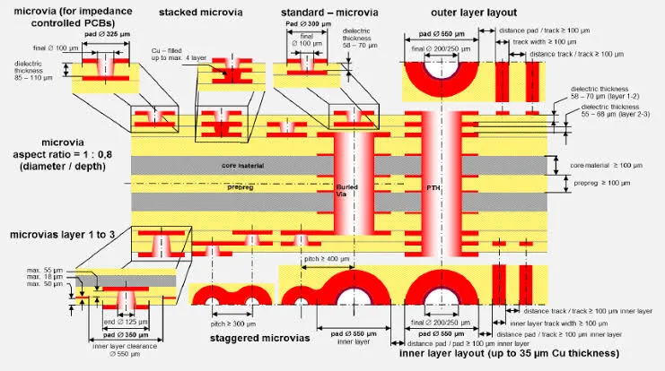
Introduction
Copper-clad laminate serves as the foundational material in PCB fabrication, providing the insulating substrate and conductive copper layers essential for circuit formation. This composite material undergoes a precise manufacturing sequence to ensure electrical reliability, mechanical strength, and compatibility with downstream processes like drilling and etching. Electrical engineers rely on high-quality copper-clad laminate manufacturing to achieve consistent signal integrity and thermal performance in electronic assemblies. Understanding the step-by-step process reveals how factory controls influence final PCB quality. This guide details each stage, drawing from standard factory practices aligned with industry specifications.
What Is Copper-Clad Laminate and Why It Matters
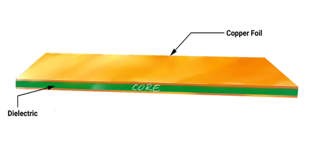
Copper-clad laminate consists of thin copper foil bonded to one or both sides of a reinforced resin substrate, forming the base for rigid or flexible printed boards. Common constructions include double-sided laminates for standard multilayer PCBs, where the substrate is typically woven glass fabric impregnated with epoxy resin. The material's properties, such as dielectric constant, peel strength, and coefficient of thermal expansion, directly impact PCB fabrication outcomes like warpage and signal loss. In high-frequency applications, low-loss variants with controlled impedance become critical. Factory-driven production ensures laminates meet performance needs for demanding environments. Engineers specify copper-clad laminates based on these attributes to optimize overall board reliability.
Its relevance extends to every PCB fabrication workflow, as defects in the laminate propagate through etching, plating, and assembly stages. Poor adhesion leads to delamination during soldering, while inconsistent thickness affects drilling accuracy. Standards like IPC-4101 define qualification criteria for base materials, guiding manufacturers on thickness tolerances and electrical tests. This alignment prevents field failures in power electronics or telecommunications gear. Selecting the right laminate type early influences cost and yield in production runs.
Raw Materials in Copper-Clad Laminate Manufacturing
Key components include reinforcing fabrics, resins, and copper foils, each processed to precise specifications. Reinforcing materials, such as alkali-free glass cloth, provide mechanical stability and dimensional control. Resins like epoxy systems are formulated for flow, cure kinetics, and flame retardancy. Copper foils come in electrodeposited or rolled annealed varieties, with the former offering uniform thickness for high-volume rigid boards. Surface treatments on foils, such as roughening or passivation, enhance resin wetting and peel strength. Factories control purity and porosity to avoid voids during lamination. The three main raw materials are reinforcing fabrics, resins, and copper foils — see our detailed guide to choosing the right copper clad laminate for material selection tips.
Glass cloth undergoes weaving and desizing before use, ensuring even resin penetration. Resin solutions incorporate hardeners, accelerators, and fillers, mixed under controlled viscosity. Copper foil thickness typically suits layer counts, with electrodeposited types dominating due to cost-effectiveness in PCB fabrication. Quality checks verify foil profile for etching compatibility. These materials set the stage for the lamination process, where integration determines laminate integrity.
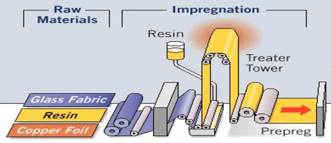
Step 1: Prepreg Preparation
Prepreg production begins the copper-clad laminate manufacturing by impregnating reinforcing fabric with resin to create a B-stage sheet. Glass cloth passes through a resin bath, where metering rolls control pickup for optimal fiber-to-resin ratio. The coated fabric then enters drying ovens, using convection or infrared heat to evaporate solvents and advance cure without full hardening. This semi-cured state allows flow during lamination while preventing premature gelation. Factories monitor gel time and tack to ensure handling ease. Visual inspection rejects sheets with foreign matter or uneven impregnation.
Vertical or horizontal treaters handle different fabrics, with tension controls preventing distortion. Resin formulation adjusts for volatility, ensuring no blistering in later presses. Post-drying, prepregs are cut to panel size and packaged in moisture-barrier bags. Storage conditions halt further cure, preserving reactivity. This step's precision affects void content and bond quality in final laminates. Engineers appreciate consistent prepreg properties for predictable multilayer builds.
Step 2: Copper Foil Preparation
Copper foil fabrication involves electrodeposition from copper sulfate solutions onto rotating drums, yielding uniform, high-purity sheets. Rolled annealed foils undergo mechanical reduction and heat treatment for ductility in flexible applications. Both types receive surface treatments like micro-roughening or oxide layers to promote resin adhesion without compromising etchability. Porosity tests confirm minimal pinholes, critical for inner layer insulation. Foils are cleaned and coated to match substrate chemistry. Factories stock profiles per IPC-4562 guidelines for foil specifications.
Treatment chemistries vary, with chromate passivation preventing oxidation during lay-up. Thickness uniformity supports fine-line etching in PCB fabrication. Electrodeposited foils suit rigid boards due to flatness, while rolled types excel in bend cycles. Quality gates include profile scans and adhesion trials. Prepared foils directly influence surface treatment efficacy post-lamination. This preparation ensures robust copper-clad laminate manufacturing outcomes.
Step 3: Lay-Up Process
Lay-up assembles prepregs and copper foils into a stack, mirroring the final laminate structure. Automated cutters shear sheets to size, followed by optical alignment on pin registers. For double-sided copper-clad laminates, operators place foil, prepreg layers, and core material in sequence, separated by caul plates. Cleanliness protocols, including tacky rollers and ionized air, eliminate contaminants that cause voids. Stack height determines press loading, with vacuum bags optional for air removal. This stage sets uniformity for the lamination process.
Multi-layer books accommodate dozens of panels, optimizing throughput. Registration accuracy prevents misalignment in multilayer PCB fabrication. Foil orientation considers grain direction for warpage control. Factories use stainless steel separators for heat transfer. Pre-lay-up checks verify sheet count and resin content. Precise lay-up minimizes resin-rich areas prone to cracking.
Step 4: Lamination Process
The lamination process cures the stack under controlled heat, pressure, and sometimes vacuum to form a monolithic copper-clad laminate. Presses with multi-platens ramp temperature gradually, allowing resin flow to wet fibers and foils before gelation. Peak conditions, tailored to resin type, dwell to achieve full cure, followed by controlled cooling to lock dimensions. Hydraulic rams apply uniform pressure, preventing porosity. Cycle times balance productivity and quality, with exhaust vents managing volatiles. This factory core step aligns with IPC-4101 performance specs. For optimal bond strength during this critical step, follow the recommendations in our article on best practices for copper cladding lamination.
Vacuum-assisted lamination reduces trapped air, enhancing dielectric integrity. Temperature profiles monitor via thermocouples for Tg achievement. Pressure gradients control flow without squeeze-out. Post-cure, panels release from the book for trimming. Variations like continuous laminators suit high-volume runs. Engineers value traceable profiles for reproducibility.
Step 5: Post-Lamination Processing, Surface Treatment, and Inspection
Trimming shears panels to size, removing flash and edges. Surface treatment options, such as light etching or Ra profiling, prepare copper for photoresist adhesion in PCB fabrication. Black oxide or alternative conversions boost peel strength for multilayer lamination. Inspections per IPC-TM-650 include peel tests, thickness mapping, and visual scans for pits or delams. Dimensional stability checks verify flatness. Packaging follows, with desiccants for storage.
Micro-etching removes oxides without base attack. Adhesion promoters ensure etch resist uniformity. Automated optical systems flag defects early. Warpage measurements guide process tweaks. This phase bridges to etching process in PCB fabrication. Quality data feeds continuous improvement.
Integration into PCB Fabrication: Etching and Beyond
Copper-clad laminates enter PCB fabrication with imaging, where photoresist coats treated surfaces. Exposure and development define circuits, followed by the etching process using ferric chloride or cupric solutions to remove unwanted copper. Spray etching ensures uniform undercut control. Post-etch stripping and differential speeding maintain line fidelity. Surface treatment like HASL or ENIG protects traces. These steps leverage laminate quality for yield.
Multilayer flows repeat lamination after inner etching. Standards guide acceptability. Engineers optimize etch factors for impedance.
Best Practices for Copper-Clad Laminate Manufacturing
Maintain cleanrooms to sub-micron levels, preventing ionic contamination. Profile presses for resin-specific ramps, avoiding fast heat-up that traps voids. Use low-profile foils for HDI density. Monitor prepreg B-stage weekly via gel time. Implement SPC on peel strength post-lam. These factory insights boost first-pass yields.
Validate lots with IPC-TM-650 suites before release. Balance cure for Tg without brittleness. Train on lay-up ergonomics. Audit suppliers for foil consistency. Such practices sustain EEAT in production.
Conclusion
Copper-clad laminate manufacturing transforms raw inputs into reliable bases for PCB fabrication through meticulous prepreg, lay-up, lamination, and inspection stages. Key processes like lamination and surface treatment ensure adhesion and etchability. Standards such as IPC-4101 and IPC-TM-650 underpin quality. Electrical engineers benefit from understanding these factory dynamics for spec selection and troubleshooting. Mastering this flow drives innovation in high-performance boards.
FAQs
Q1: What is the lamination process in copper-clad laminate manufacturing?
A1: The lamination process involves stacking prepregs and copper foils, then applying heat and pressure in a multi-platen press to cure the resin and bond layers. Precise temperature ramps control flow and gelation, while vacuum options minimize voids. Cooling locks structure. This step ensures void-free integrity per IPC-4101, critical for PCB fabrication reliability. Factories tailor cycles for resin types.
Q2: How does surface treatment affect copper-clad laminate in PCB fabrication?
A2: Surface treatment on copper foils or post-lam panels enhances adhesion for photoresist and multilayer bonding. Roughening or oxide layers improve peel strength without etch hindrance. It prevents delamination during thermal stress. Engineers select profiles for fine-line compatibility. Proper treatment boosts yield in etching process.
Q3: What role does the etching process play after copper-clad laminate production?
A3: The etching process removes excess copper post-imaging to form circuits on the laminate. Chemical sprays dissolve unprotected areas uniformly. Timing controls sidewall quality. It follows surface treatment for clean lines. This integrates CCL into full PCB fabrication, demanding laminate flatness.
Q4: Why control prepreg quality in copper-clad laminate manufacturing?
A4: Prepreg quality dictates resin flow, void content, and bond strength in lamination. Consistent B-stage prevents under-cure or brittleness. Factories test gel time and volatiles. It ensures dielectric uniformity for signal integrity. Poor control risks warpage in multilayer builds.
References
IPC-4101 - Specification for Base Materials for Rigid and Multilayer Printed Boards. IPC
IPC-TM-650 - Test Methods Manual. IPC
IPC-4562 - Requirements for Copper Foil for Printed Boards. IPC