Introduction
Scaling the PCB manufacturing process from prototype to mass production introduces significant engineering challenges, particularly for glass-reinforced PCBs. These boards use woven glass fabrics embedded in resin matrices to provide superior mechanical strength, dimensional stability, and resistance to thermal stresses compared to paper-based alternatives. Electric engineers must address variations in material properties, process repeatability, and yield rates as production volumes increase from dozens to thousands of units. Glass PCB manufacturing relies on precise control of lamination, drilling, and plating steps to prevent defects like delamination or warpage that can escalate costs in high-volume runs. This article details the PCB manufacturing process, scaling PCB production strategies, and integration with PCB assembly for reliable mass production PCB outcomes. By following factory-driven best practices, teams can achieve consistent quality while minimizing downtime and waste.
Understanding Glass-Reinforced PCBs in Modern Electronics
Glass-reinforced PCBs form the backbone of most rigid board applications due to their balance of electrical performance and robustness. The reinforcement typically involves E-glass woven fabrics impregnated with epoxy resin, creating laminates that withstand soldering temperatures and mechanical handling. In the context of scaling PCB production, these materials must exhibit low coefficient of thermal expansion to match component requirements during PCB assembly. Factory processes prioritize uniform glass distribution to avoid voids or resin-rich areas that compromise signal integrity. Relevance grows in mass production PCB scenarios where high layer counts demand tight control over thickness uniformity and bow and twist. Engineers appreciate how glass reinforcement enables higher circuit densities without sacrificing reliability.
Core Elements of the PCB Manufacturing Process for Glass-Reinforced Boards
The PCB manufacturing process begins with material preparation, where glass fabric styles per IPC-4412C specifications are selected based on yarn count and weave tightness for optimal resin flow. Prepregs, partially cured resin sheets with embedded glass fibers, are cut and stacked with copper foils to form panel layups matching the desired multilayer configuration. Hydraulic pressing applies heat and pressure to fully cure the stack, bonding layers while minimizing voids through controlled vacuum and ramp rates. Post-lamination, drilling creates vias with high-precision CNC machines, followed by desmear to remove epoxy residue exposing glass fibers for plating adhesion. Electroless copper deposition initiates barrel plating, building conductive paths resistant to high-current densities in mass production. Etching defines traces, and final imaging applies solder mask over the glass-reinforced base for protection.
This sequence ensures the structural integrity essential for scaling PCB production. Variations in glass fabric thickness directly impact drill bit life and hole wall quality, requiring statistical process control in volume runs. Surface preparation after desmear becomes critical to prevent plating skips on exposed glass ends.
Challenges in Scaling Glass PCB Manufacturing for Mass Production
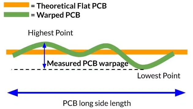
Transitioning to mass production PCB amplifies issues like warpage from asymmetric glass reinforcement in multilayer stacks. Prototype runs tolerate minor bow due to low volumes, but high yields demand balanced layups with symmetric core and prepreg counts. Material variability, such as resin content fluctuations in glass prepregs, leads to inconsistent dielectric thickness, affecting impedance control at scale. Drilling throughput bottlenecks emerge as panel sizes increase, with glass fibers accelerating tool wear and necessitating frequent replacements. Plating uniformity suffers under high current loads, risking overplating on inner layers or underplating vias. These factors drive yield drops from over 95 percent in prototypes to below 90 percent without optimization, inflating costs. Material qualification is critical—see our complete guide on CEM-1 vs. FR-4: Choosing the Right PCB Material for Your Project.
Engineers must also consider environmental controls, as humidity affects glass moisture absorption, potentially causing popcorning during reflow in PCB assembly. Supply chain reliability for consistent glass fabric lots prevents batch-to-batch discrepancies.
Best Practices for Scaling PCB Production
To overcome scaling hurdles, implement design for manufacturability early by specifying glass styles suited to layer count and panel utilization. Optimize panel arrays for maximum yield, incorporating breakaway tabs and fiducials for automated handling. Transition to statistical process control, monitoring key variables like press temperature profiles and plating bath chemistry in real time. For glass PCB manufacturing, qualify laminates per IPC-6012F qualification and performance specifications to ensure they meet class 3 requirements for high-reliability applications. Automate drilling with adaptive feeds to extend tool life on glass-filled materials, targeting hole location tolerances under 0.075 mm. Introduce inline optical inspection post-etch to catch defects before solder mask application. For advanced stack-up strategies, review our HDI PCB Assembly: The Ultimate Guide to Materials, Stack-Up Structures, DFM Best Practices.
In PCB assembly preparation, bake boards to remove absorbed moisture from glass reinforcement, preventing voids during reflow. Collaborate with assembly partners on stencil design for uniform paste deposition over fine-pitch traces.
Quality Control Measures in Mass Production PCB
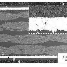
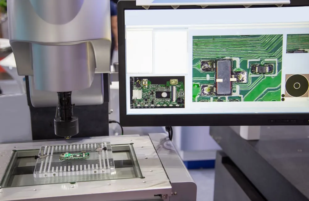
Quality assurance shifts from visual checks in prototypes to automated systems in mass production. IPC-A-600M acceptability criteria guide inspections for conductor spacing, hole registration, and laminate voids visible in glass-reinforced cross-sections. Electrical testing verifies continuity and shorts at full production speeds, using flying probe or bed-of-nails fixtures. Thermal stress screening simulates assembly reflow, detecting delaminations at glass-resin interfaces. Solderability preservation through hot air solder leveling or organic solderability preservatives maintains joint reliability. Data analytics from these steps feed back into process adjustments, sustaining yields above 98 percent.
Traceability via embedded barcodes on panels links defects to specific glass lots, enabling root cause analysis.
Integrating PCB Assembly in Scaled Glass PCB Manufacturing
PCB assembly scales alongside board fabrication, with glass-reinforced substrates influencing pick-and-place accuracy due to their rigidity. Surface mount technology lines handle high volumes, but glass-induced surface roughness requires precise stencil apertures to avoid bridging. Reflow profiles account for the higher thermal mass of glass epoxy, extending soak times for uniform wetting. Through-hole components demand controlled wave soldering to prevent glass fiber damage from flux residues. Final functional testing confirms assembly integrity under vibration, leveraging the mechanical strength of glass reinforcement. Seamless handoff from fabrication to assembly minimizes handling-induced warpage.
Conclusion
Scaling glass PCB manufacturing from prototype to mass production demands a holistic approach encompassing material selection, process optimization, and rigorous quality controls. Key to success lies in adhering to standards like IPC-4412C for glass fabrics, ensuring consistency across the PCB manufacturing process. Engineers benefit from proactive DFM, automation, and data-driven refinements to achieve high yields in mass production PCB runs. PCB assembly integration further solidifies reliability, enabling deployment in demanding applications. By mastering these elements, teams transition smoothly, reducing time-to-market and costs while upholding performance.
FAQs
Q1: What are the main challenges in the PCB manufacturing process for glass-reinforced boards during scaling PCB production?
A1: Glass PCB manufacturing faces issues like warpage from thermal mismatches, drill wear on fibers, and plating uniformity at high volumes. Maintaining consistent prepreg resin content prevents voids, while balanced layups control bow and twist. Automated controls and qualified materials per industry standards address these for reliable mass production PCB. Factory monitoring ensures yields stay high.
Q2: How does glass reinforcement impact PCB assembly in mass production?
A2: Glass fibers provide rigidity, aiding pick-and-place accuracy but requiring moisture baking to avoid reflow defects. Solder mask over rough surfaces needs precise stenciling for paste release. Thermal profiles extend for epoxy's mass, ensuring joint integrity. This supports high-speed lines in scaling PCB production without quality loss.
Q3: What role do standards play in glass PCB manufacturing for mass production PCB?
A3: Standards define fabric specs, qualification tests, and acceptability, guiding consistent processes. They minimize variability in lamination and plating, crucial for volume yields. Compliance verifies performance under assembly stresses, reducing field failures. Engineers rely on them for factory-driven scaling PCB production.
Q4: Why is quality control critical when scaling from prototype to mass production PCB?
A4: High volumes amplify defect costs, so inline inspections catch laminate flaws early. Electrical and thermal tests validate glass-reinforced integrity. Analytics optimize processes, sustaining efficiency. This ensures PCB assembly readiness and long-term reliability.
References
IPC-4412C - Specification for Finished Fabric Woven from E-Glass Yarns. IPC.
IPC-6012F - Qualification and Performance Specification for Rigid Printed Boards. IPC, 2023.
IPC-A-600M - Acceptability of Printed Boards. IPC, 2025.


