Introduction
In the evolving landscape of printed circuit manufacturing, fine line screen printing stands out as a pivotal technique for producing high-resolution printed electronics. This method enables the deposition of conductive inks with exceptional precision, supporting denser circuit patterns on flexible and rigid substrates alike. Electrical engineers increasingly rely on advanced screen printing techniques to meet demands for compact, reliable devices in applications ranging from wearables to sensors. Fine line silkscreen pushes the boundaries of resolution, allowing traces and features that rival photolithographic processes while maintaining cost-effectiveness in production. As printed electronics advance, mastering this art becomes essential for optimizing performance and manufacturability. Factory insights reveal that consistent high-resolution outcomes depend on meticulous control over materials and processes.
What Is Fine Line Silkscreen?
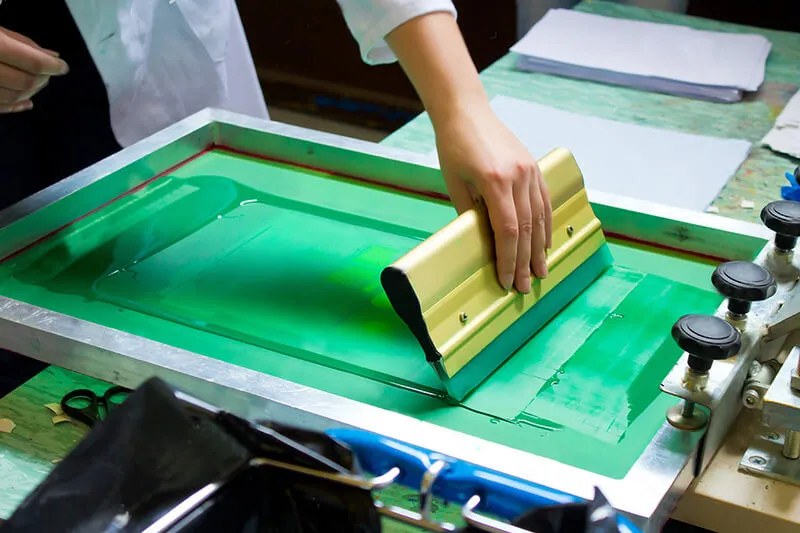
Fine line screen printing, often referred to as fine line silkscreen in printed electronics contexts, involves forcing conductive ink through a finely meshed screen onto a substrate to form intricate patterns. The process uses a stencil created on the screen to define the printed areas, where ink passes through open apertures while blocked elsewhere. This technique differs from traditional silkscreen on PCBs, which primarily applies non-conductive legend inks, by focusing on electrically functional layers with conductive ink printing. High-resolution printed electronics demand meshes with high thread counts and thin wires to achieve sharp edges and minimal spreading. Engineers appreciate how this method scales from prototypes to high-volume printed circuit manufacturing without specialized cleanroom environments. The result is durable circuitry integral to modern flexible electronics.
Why Fine Line Screen Printing Matters in Printed Circuit Manufacturing
High-resolution printed electronics enable smaller form factors and higher component densities, critical for next-generation devices constrained by space. Fine line screen printing reduces material waste compared to etching-based methods, aligning with sustainable manufacturing goals in PCB production. It supports rapid iteration, as screens can be quickly modified for design changes, accelerating time-to-market for electrical engineers. Conductive ink printing via this technique accommodates diverse substrates like polyimide films or glass, expanding applications in automotive and medical sectors. Factory-driven processes highlight its throughput advantages, producing thousands of units per hour with consistent quality. Ultimately, mastering advanced screen printing techniques ensures compliance with performance specs while lowering costs.
Technical Principles of Fine Line Silkscreen
The core of fine line screen printing lies in the interplay between screen construction, ink rheology, and printing dynamics. Screens feature high-tension meshes coated with photoemulsion, where ultraviolet exposure hardens areas outside the pattern, creating precise stencils. Conductive inks, formulated with metal particles suspended in binders, must exhibit pseudoplastic behavior to shear-thin under pressure and recover viscosity post-print. During printing, a squeegee sweeps across the screen at controlled angles and speeds, controlling ink transfer volume and minimizing distortion. Snap-off distance, the gap between screen and substrate, prevents smearing while ensuring clean release. These principles allow advanced screen printing techniques to produce features with sharp definition, vital for signal integrity in high-resolution printed electronics.
Mesh selection profoundly influences resolution in conductive ink printing. Finer threads and higher counts reduce aperture size, limiting ink flow to tighter patterns. Emulsion thickness and resolution determine stencil wall profiles, impacting ink deposition uniformity. Ink particle size must align with feature dimensions to avoid clogging or rough edges. Substrate surface energy affects wetting, where plasma treatments enhance adhesion without compromising conductivity. Factory experience shows that optimizing these elements per IPC-A-600 acceptability criteria yields reliable layers across production runs.
Suggested Reading: Silkscreen Design for High Density PCBs: Achieving Clarity in Compact Spaces
Advanced Screen Printing Techniques for High Resolution
Several refinements elevate standard screen printing to advanced levels for printed electronics. Electroformed nickel stencils offer superior edge definition over traditional emulsions, reducing undercutting in fine features. High-tension frames minimize deflection during printing, maintaining registration accuracy across large substrates. Multi-pass printing builds thicker conductive layers, enhancing current-carrying capacity without sacrificing resolution. Vacuum-assisted tables hold flexible substrates flat, countering warpage during ink curing. These techniques, combined with precise environmental controls like humidity and temperature, enable conductive ink printing at densities suitable for RF circuits. Electrical engineers benefit from their scalability in printed circuit manufacturing setups.
Registration systems using fiducials and optical alignment ensure layer-to-layer precision, crucial for multilayer high-resolution printed electronics. Rheology modifiers in inks prevent settling, sustaining print quality over extended runs. Post-print sintering, via infrared or convection ovens, densifies particles for optimal conductivity. Advanced screen printing techniques also incorporate hybrid approaches, like combining screen with aerosol jet for ultra-fine vias. Standards such as IPC-6012 guide qualification, verifying performance under thermal and mechanical stress. Factory protocols emphasize validation through cross-sections and resistance measurements.
Best Practices for Achieving High Resolution in Conductive Ink Printing
Start with ink-substrate compatibility testing to predict spreading or dewetting issues. Select meshes matched to ink viscosity, balancing resolution with throughput. Maintain squeegee durometer and pressure within narrow tolerances to avoid flooding or starvation. Clean screens ultrasonically between runs to prevent ghosting. Implement inline inspection for defects like pinholes or bridges, using automated optical systems. Document process windows, adjusting for batch variations in ink lots. These practices, rooted in factory-driven optimization, support consistent fine line screen printing outcomes.
Curing profiles must align with ink specifications, avoiding oxidation that degrades conductivity. Handle substrates with anti-static measures to prevent particle contamination. For high-volume printed circuit manufacturing, automate squeegee paths and ink dispensing for repeatability. Collaborate with suppliers on custom formulations tailored to target resolutions. Adherence to IPC-2221 design guidelines ensures silkscreen and conductive layers coexist without interference. Regular calibration of printing equipment sustains long-term precision.
Suggested Reading: Silkscreen Placement: Optimizing Space in Compact PCB Designs
Troubleshooting Common Challenges in Fine Line Silkscreen
Ink bleeding often stems from excessive snap-off or high humidity, resolved by drying screens pre-print. Poor adhesion on low-energy substrates improves with corona treatment, enhancing ink wetting. Misregistration in multilayer builds corrects via fiducial-based alignment tweaks. Pinholes from air entrapment diminish with degassed inks and slower squeegee speeds. Conductivity variability post-cure indicates incomplete sintering, addressed by profiled heating ramps. Factory troubleshooting logs track root causes, applying statistical process control for prevention. These insights empower engineers to refine advanced screen printing techniques iteratively.
Conclusion
Fine line screen printing represents a cornerstone of high-resolution printed electronics, blending artistry with engineering precision. By understanding technical principles and implementing best practices, electrical engineers can unlock denser, more reliable circuits in printed circuit manufacturing. Conductive ink printing's versatility supports innovation across industries, from rigid PCBs to flexible hybrids. Standards like IPC guidelines ensure quality and interoperability. As demands for miniaturization grow, mastering these techniques will define competitive edges in production. Prioritize process control and material synergy for sustained excellence.
FAQs
Q1: What is fine line screen printing in the context of high-resolution printed electronics?
A1: Fine line screen printing uses high-thread-count meshes and precise stencils to deposit conductive inks with sharp, narrow features on substrates. This advanced screen printing technique achieves resolutions suitable for dense circuitry, outperforming traditional methods in flexibility. Factory processes emphasize ink rheology and printing parameters for consistent results. It integrates seamlessly into printed circuit manufacturing workflows. (52 words)
Q2: How do advanced screen printing techniques improve conductive ink printing?
A2: Advanced techniques like high-tension screens and electroformed stencils minimize distortion, enabling finer lines in conductive ink printing. Controlled squeegee dynamics and registration systems ensure layer accuracy for multilayer high-resolution printed electronics. Environmental controls prevent defects, boosting yield. Electrical engineers apply these for reliable performance in demanding applications. (58 words)
Q3: What role do industry standards play in fine line silkscreen quality control?
A3: Standards such as IPC-A-600 define acceptability criteria for printed features, guiding inspection in fine line screen printing. They specify tolerances for edge definition and adhesion in printed circuit manufacturing. Compliance verifies durability under operational stresses. Factory teams use them to standardize processes across production. (54 words)
Q4: Why is substrate preparation critical for high-resolution printed electronics?
A4: Proper substrate preparation, including surface treatments, optimizes ink adhesion and prevents spreading in fine line screen printing. It ensures uniform deposition for conductive paths. Cleanliness controls contamination risks. This step enhances overall resolution and reliability in advanced applications. (48 words)
References
IPC-A-600K — Acceptability of Printed Boards. IPC, 2020
IPC-6012E — Qualification and Performance Specification for Rigid Printed Boards. IPC, 2017
IPC-2221 — Generic Standard on Printed Board Design. IPC, 2012


