Introduction
Printed circuit boards form the backbone of modern electronics, where even minor defects can lead to system failures with significant financial repercussions. Electrical testing stands as a critical gatekeeper in the manufacturing process, verifying continuity, isolation, and overall integrity before assembly proceeds. Among testing methods, flying probe testing offers unique flexibility, particularly for prototypes and low-volume production. This article examines the ROI of PCB testing through flying probe technology, focusing on flying probe testing cost analysis and the cost-benefit of flying probe systems. By understanding these elements, electrical engineers can better justify PCB test spend in their quality control strategies. Factory-driven insights reveal how this investment aligns with long-term production efficiency.
What Is Flying Probe Testing?
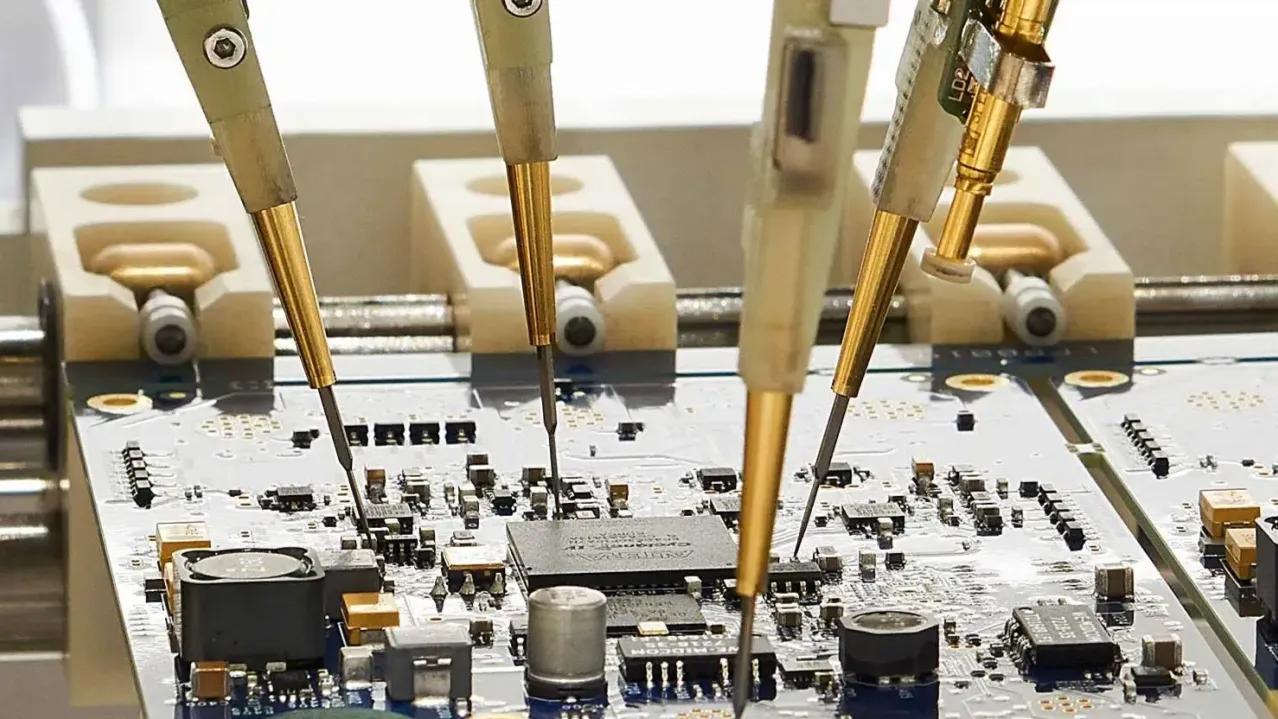
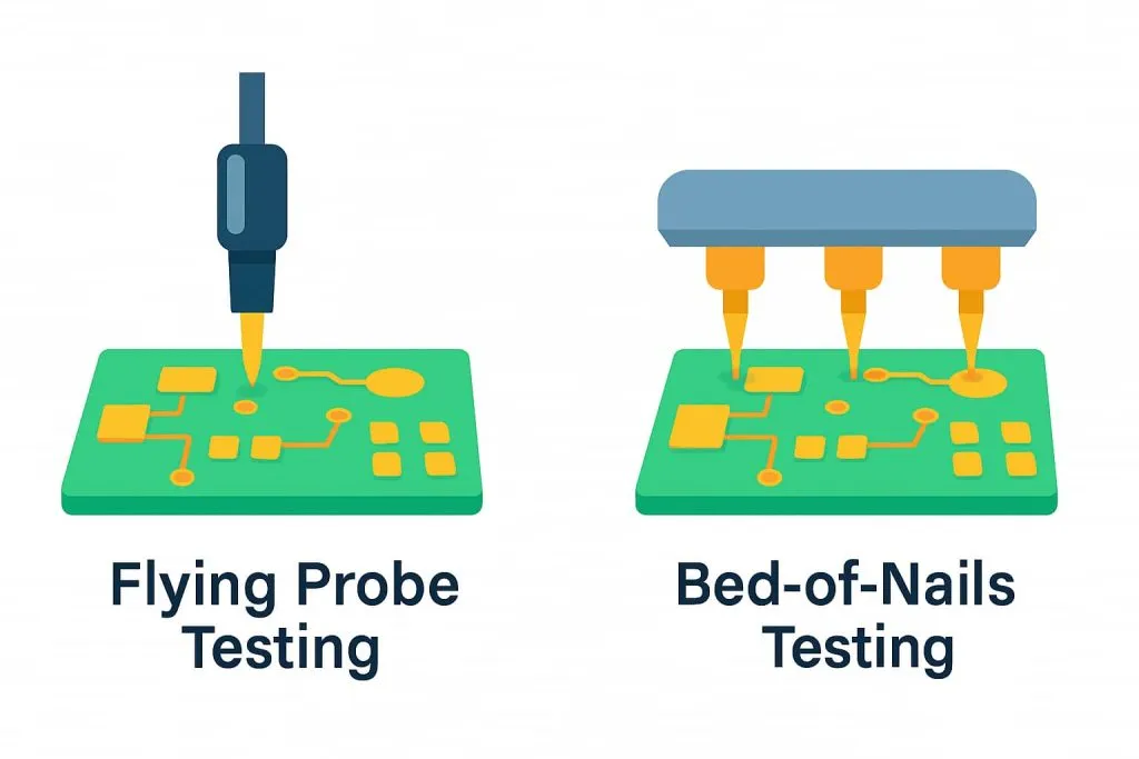
Flying probe testing is a fixtureless electrical test method that employs movable probes to contact test points on a bare PCB or assembled board. Unlike traditional bed-of-nails systems, which require custom fixtures, flying probe testers use computer-controlled probes that "fly" to specified locations based on CAD data. This approach enables rapid test program generation, often within hours, making it ideal for new product introductions. The system detects opens, shorts, resistance deviations, and capacitance issues by measuring electrical parameters at nets and vias. Engineers appreciate its adaptability to high-density boards with fine-pitch components. Compliance with standards like IPC-6012E ensures that tested boards meet qualification and performance specifications for rigid printed boards.

Why Flying Probe Testing Matters for PCB Quality Control
In PCB manufacturing, undetected electrical faults propagate to assembly and field deployment, escalating costs exponentially. Flying probe testing addresses this by providing comprehensive netlist verification without physical constraints of fixtures. It excels in scenarios with frequent design changes, where retooling fixtures proves impractical and expensive. Factory processes benefit from its high fault coverage, typically matching or exceeding fixture-based methods for accessible points. This method supports quality objectives outlined in ISO 9001:2015, emphasizing consistent process control and defect prevention. Ultimately, integrating flying probe enhances yield rates and reduces escape defects, directly impacting the bottom line.
Technical Principles of Flying Probe Testing
Flying probe systems rely on precision mechanics and advanced software to position probes with micron-level accuracy. Typically, four to eight probes operate simultaneously, alternating between top and bottom sides of the board. Test algorithms employ vectorless or guided probing, where guided tests follow predefined nets while vectorless scans detect unprogrammed faults via adjacency analysis. Contact force and dwell time are calibrated to avoid board damage, ensuring repeatability across panels. Electrical measurements use low-voltage DC for continuity and high-voltage for isolation, aligning with guidelines in IPC-9252B for electrical test methods. These principles enable reliable detection of subtle issues like insufficient plating or drill breakout.
The software interface imports Gerber and netlist files, automatically generating probe paths while optimizing for speed. Collision avoidance algorithms prevent probe interference on densely routed boards. Advanced models incorporate vision systems for fiducial alignment and component presence checks. This technical foundation supports testing of multilayer boards up to stringent class 3 requirements. Engineers can customize test thresholds based on material properties and layer counts. Such capabilities make flying probe a staple in quality-focused factories.
Flying Probe Testing Cost Analysis: Upfront and Ongoing Expenses
Evaluating the flying probe testing cost analysis begins with capital investment in the tester itself, which represents a substantial initial outlay compared to manual methods. Programming and setup costs remain low due to software automation, eliminating fixture fabrication expenses that plague bed-of-nails systems. Operational costs include probe maintenance, as wear from repeated contacts necessitates periodic replacements, and electricity for high-speed movements. Throughput time per board influences labor costs, with test durations scaling based on net count and board complexity. Factory data shows these costs stabilize over time with preventive maintenance schedules. Engineers must factor in training for operators to maximize uptime and efficiency.
Variable costs arise from panel size and test coverage depth, where denser probing increases cycle time. Integration with handling systems adds to the total but improves automation flow. Compared to outsourcing testing, in-house flying probe reduces per-board fees for recurring builds. Long-term analysis reveals amortization of upfront costs through internal efficiencies. This breakdown aids in justifying PCB test spend during budget reviews. Overall, the structure favors operations with variable production volumes.
The Cost-Benefit of Flying Probe: Advantages Over Fixture-Based Testing
The cost-benefit of flying probe shines in its elimination of fixture-related expenses, which can dominate budgets for prototype runs. Custom fixtures demand engineering time, materials, and machining, often delaying production by weeks. Flying probe bypasses this, enabling same-day testing post-design freeze. It achieves comparable fault coverage for most nets, with adjacency testing filling gaps in inaccessible areas. Reduced scrap from early detection lowers material waste and rework labor. Factories report faster time-to-market as a key intangible benefit.
For high-mix environments, flying probe's flexibility outweighs slower per-board speeds versus parallel fixture testing. In low-volume scenarios, its ROI surpasses alternatives by avoiding underutilized fixture investments. Enhanced data logging supports root-cause analysis, preventing recurring defects. This method scales well for double-sided and multilayer boards common in electrical engineering applications. Yield improvements compound savings across production lifecycles. Thus, the cost-benefit justifies adoption where adaptability trumps raw speed.
Calculating the ROI of PCB Testing with Flying Probe
To compute the ROI of PCB testing, engineers start by quantifying tangible gains like scrap reduction and yield uplift against total ownership costs. Basic formula considers net savings from avoided failures divided by investment, tracked over a payback horizon of two to three years. Key inputs include baseline defect rates pre- and post-implementation, derived from factory SPC data. Intangibles such as accelerated prototyping cycles contribute to faster revenue realization. Sensitivity analysis varies volume assumptions to model low- versus high-mix scenarios. This structured approach strengthens proposals for capital approval.
Software tools simulate scenarios by inputting test coverage, fault escape probabilities, and rework costs. Higher initial detection correlates with downstream assembly savings. For instance, catching opens early prevents populated board scrapping. Cumulative effects amplify ROI in multi-project pipelines. Electrical engineers leverage this for data-driven decisions. Regular reviews refine models with actual performance metrics.
Best Practices for Justifying PCB Test Spend
Select flying probe when production volumes fall below thresholds where fixture costs amortize, typically prototypes to mid-volume. Pair it with optical inspection for hybrid coverage, maximizing defect capture. Establish test specifications per IPC-6012E to ensure class-appropriate verification. Train teams on probe calibration and data interpretation to sustain accuracy. Monitor key metrics like first-pass yield and false calls to optimize programs. Document savings quarterly to build case for expansions.
Integrate flying probe into the quality management system per ISO 9001:2015 for auditable processes. Use netlist comparisons to validate test programs against design. Schedule maintenance during off-peaks to minimize downtime. Collaborate with design teams for test-point optimization early in layout. These practices solidify the business case for investment.
Real-World Insights: Maximizing ROI in Factory Settings
In a typical factory handling diverse PCB types, flying probe proves invaluable for rapid iterations on high-density designs. One scenario involves transitioning prototypes to pilot runs, where fixture delays previously bottlenecked schedules. Implementing flying probe cut lead times, enabling quicker customer feedback loops. Defect data pinpointed plating inconsistencies, addressed via supplier audits. Yield climbed steadily, offsetting tester utilization. Such outcomes underscore factory-driven ROI realization.
For complex multilayer boards, flying probe's vectorless capabilities caught latent shorts missed by simpler methods. Integration with MES systems provided real-time analytics for process tweaks. Engineers noted reduced field returns, bolstering reliability reputation. These insights guide when to deploy flying probe versus alternatives. Consistent application yields compounding benefits.
Conclusion
Flying probe testing delivers strong ROI through fixture savings, flexibility, and superior early defect detection. Its cost-benefit of flying probe aligns perfectly with modern manufacturing demands for agility and quality. By conducting thorough flying probe testing cost analysis, teams can confidently justify PCB test spend. Adhering to standards like IPC-9252B ensures reliable outcomes. Electrical engineers stand to gain from higher yields and faster cycles. Investing in this technology fortifies PCB quality control for competitive advantage.
FAQs
Q1: What does flying probe testing cost analysis typically reveal for low-volume PCB production?
A1: Flying probe testing cost analysis highlights low setup expenses due to fixtureless operation, making it economical for prototypes and runs under a thousand boards. It offsets higher per-board test times with savings on custom tooling and rapid programming. Factories see payback through scrap reduction and yield gains. This approach suits variable production, per quality standards integration.
Q2: How do you calculate the ROI of PCB testing using flying probe systems?
A2: Calculate ROI of PCB testing by subtracting total costs from benefits like rework avoidance and yield improvements, then dividing by investment. Track metrics over 24-36 months, factoring throughput and fault coverage. Factory data refines accuracy. Sensitivity to volume changes validates decisions for electrical engineers.
Q3: When is the cost-benefit of flying probe most favorable compared to fixture testing?
A3: The cost-benefit of flying probe excels in high-mix, low-volume scenarios where fixture costs outweigh test speed advantages. It supports design changes without retooling, ideal for NPI. For complex boards, its accessibility boosts coverage. Standards compliance ensures quality parity.
Q4: What role does justifying PCB test spend play in factory quality control?
A4: Justifying PCB test spend involves demonstrating yield uplifts and failure cost reductions via data. Flying probe fits ISO 9001:2015 by enabling consistent verification. Engineers use it for prototypes, scaling ROI through process integration. Long-term savings justify the strategic outlay.
References
IPC-6012E - Qualification and Performance Specification for Rigid Printed Boards. IPC, 2017
IPC-9252B - Electrical Test Guidelines. IPC, 2018
ISO 9001:2015 - Quality Management Systems. ISO, 2015


