Introduction
In high-speed PCB designs, signal integrity challenges often emerge not just from the initial layout but from manufacturing variations that alter electrical performance. Engineers investing significant time in simulations may still face issues like signal reflections or crosstalk when prototypes arrive from the fabricator. This gap between design intent and production reality drives up PCB rework costs, sometimes exceeding 20% of project budgets in complex assemblies. Design for manufacturability, or DFM, applied specifically to signal integrity, bridges this divide through early collaboration with manufacturers. By integrating manufacturer feedback during the design phase, teams can preempt signal integrity issues in manufacturing, ensuring reliable performance from first-pass builds. This approach not only minimizes costly reworks but also accelerates time-to-market for electric engineers tackling gigabit-speed interfaces.
Understanding DFM for Signal Integrity
DFM for signal integrity refers to the practice of designing PCBs with manufacturing processes and tolerances in mind to preserve controlled impedance, minimize crosstalk, and maintain timing margins. Traditional DFM focuses on basic fabricability like drill sizes and panelization, but PCB design for manufacturability signal integrity extends to electrical parameters influenced by production variables. For instance, trace etch tolerances directly impact characteristic impedance, while layer stack-up variations affect dielectric constants. Manufacturers provide stack-up charts and process capabilities that designers must reference early to align simulations with real-world outcomes. Without this, even meticulously simulated designs falter, leading to high PCB rework costs from yield losses or field failures. Electric engineers benefit from viewing DFM as an iterative loop between design tools and fab data.
Why Signal Integrity Matters in Manufacturing Collaboration
Signal integrity issues in manufacturing arise because production introduces variability that simulations rarely fully capture, such as copper plating thickness or material anisotropy. High-speed signals demand precise 50-ohm or 100-ohm impedances, yet a 10% deviation in trace width can shift these values by 5-10 ohms, causing eye diagram closure. Early DFM signal integrity collaboration allows engineers to validate design rules against fab capabilities, preventing these mismatches. Procurement teams often overlook this until NPI stages, resulting in scrapped panels and rushed redesigns. By involving manufacturers upfront, teams reduce risks associated with via transitions, where drill smear or plating voids degrade return paths. Ultimately, this proactive stance upholds product reliability in applications like data centers or automotive electronics.
Key Causes of Signal Integrity Issues from Manufacturing Variations
Manufacturing processes introduce several variables that compromise signal integrity, starting with conductor geometry control. Etch processes, governed by panel processing and chemistry, can vary trace widths by several microns, altering impedance profiles across the board. In multilayer stacks, dielectric thickness inconsistencies from lamination pressure lead to propagation delay skews, critical for DDR memory interfaces. Via fabrication adds further challenges, as aspect ratios exceeding 10:1 risk incomplete plating, creating stubs that reflect high-frequency energy. Material properties like glass transition temperature influence dimensional stability during reflow, exacerbating crosstalk in dense routing. These factors highlight why PCB design for manufacturability signal integrity must incorporate fab-specific tolerance data from the outset.

Copper surface roughness, another manufacturing artifact, increases insertion loss at frequencies above 5 GHz by enhancing skin effect losses. While designers specify low-loss dielectrics, fab choices in foil types can introduce unintended roughness. Layer-to-layer registration errors misalign reference planes, weakening shielding and amplifying EMI susceptibility. Solder mask application over traces modifies effective capacitance, a subtlety often missed in pre-fab reviews. Thermal expansion mismatches during assembly further distort geometries, impacting differential pair lengths. Addressing these requires DFM signal integrity collaboration to map design margins against process windows.
Technical Principles Behind DFM-SI Alignment
Controlled impedance relies on the transmission line model, where Z0 = sqrt(L/C), directly tied to trace width, height, and dielectric constant. Manufacturing tolerances on these parameters demand design margins, such as specifying nominal widths with +/-5% allowances. Time-domain reflectometry principles guide verification, but fab test coupons embedded in panels provide empirical data. Crosstalk mitigation follows coupling equations, where aggressive spacing rules must account for etch undercut. Return path integrity, per ground plane rules, suffers from breakout routing variances. Electric engineers apply these principles by simulating worst-case fab scenarios early.
Via optimization embodies DFM principles, distinguishing blind, buried, and through vias based on stub length impacts. Stubs shorter than lambda/10 at the knee frequency minimize reflections, but drill depth control ensures compliance. Material DK variation, typically 1-2% across a sheet, skews phase velocities in length-matched pairs. IPC-6012E outlines qualification for rigid boards, emphasizing conductor width and spacing tolerances critical for high-speed performance. Lamination cycles affect prepreg flow, influencing final thicknesses. These mechanisms underscore the need for stack-up reviews in design reviews.
Best Practices for DFM Signal Integrity Collaboration
Early engagement starts with sharing Gerber files and stack-ups during schematic capture, allowing manufacturers to flag impedance mismatches. Establish design rulesets incorporating fab DFM guidelines, like minimum annular ring sizes for high-aspect vias. Conduct joint webinars or calls to discuss routing densities against panel yield models. Embed test structures for TDR and cross-talk measurements in coupon areas. Release control impedance targets with tolerance bands, verified post-fab. This DFM signal integrity collaboration cuts iteration cycles significantly.
A comprehensive PCB design review checklist ensures thoroughness. Key items include verifying trace width tolerances against etch charts, confirming layer thickness stack-ups match DK simulations, and checking via back-drill specs for stub removal. Review spacing for crosstalk budgets under worst-case coupling lengths, assess breakout fanouts for ground stitching density, and validate material specs for loss tangent at operating frequencies. Simulate thermal warpage effects on bow and twist, ensuring compliance with flatness specs. Cross-reference with IPC-A-600K acceptability criteria for conductor features. Table 1 outlines a sample checklist.
- Impedance Control - Specify width/height - Etch tolerance charts
- Via Integrity - Aspect ratio <10:1 - Drill/plating capabilities
- Stack-up - DK/Er variation - Lamination thickness data
- Crosstalk - Spacing >3x height - Registration accuracy
- Loss Budget - Roughness factor - Foil type options

Iterate via DFMA tools internally before fab quote, then refine with vendor feedback. Prototype small panels for SI characterization before full runs. Document lessons in a shared repository for future projects. These practices directly lower PCB rework costs by catching issues pre-tooling.
Real-World Insights from Troubleshooting SI Failures
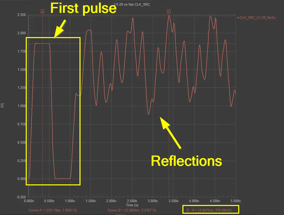
In one scenario, a 10-layer board with PCIe Gen4 lanes exhibited eye height degradation post-assembly, traced to 15% dielectric thickness variation from uneven lamination. Early collaboration would have prompted filled vias or tighter press cycles. Another case involved crosstalk spikes from misregistered planes, resolved by adjusting drill fiducials. J-STD-001D soldering requirements highlight assembly impacts on SI, like pad cratering affecting launch points. Troubleshooting oscilloscope captures and VNA sweeps reveal fab-induced anomalies. Insights emphasize baseline fab audits for process Cpks on critical features.
Conclusion
DFM for signal integrity transforms potential pitfalls into robust designs through proactive manufacturer partnerships. By prioritizing PCB design for manufacturability signal integrity, electric engineers sidestep common signal integrity issues in manufacturing and curb escalating PCB rework costs. Implementing a PCB design review checklist and embedding test structures fosters alignment between design and production. Standards like IPC-6012E and IPC-A-600K provide the framework for tolerance expectations. Ultimately, this collaboration yields first-pass success, reliable performance, and cost efficiencies across high-speed applications.
FAQs
Q1: What are the main signal integrity issues in manufacturing that DFM addresses?
A1: Signal integrity issues in manufacturing, such as impedance discontinuities from etch variations and crosstalk from layer misalignment, are mitigated by PCB design for manufacturability signal integrity practices. Early DFM signal integrity collaboration incorporates fab tolerances into simulations, ensuring margins for dielectric thickness and via plating. This prevents reflections and timing skews common in high-speed boards. Engineers verify via test coupons for real-world correlation.
Q2: How does early DFM signal integrity collaboration reduce PCB rework costs?
A2: DFM signal integrity collaboration upfront shares stack-ups and rulesets, identifying issues like via stubs or roughness impacts before tooling. This avoids scrapped prototypes and assembly failures, directly cutting PCB rework costs tied to yield losses. Manufacturers provide process data for worst-case modeling, streamlining iterations. Resulting first-pass yields improve project economics for electric engineers.
Q3: What should a PCB design review checklist for signal integrity include?
A3: A PCB design review checklist must cover trace geometries with fab tolerances, stack-up DK variations, via aspect ratios, and spacing for coupling budgets. Include ground plane continuity checks and material loss specs. Cross-reference against standards for acceptability. This ensures DFM signal integrity collaboration catches manufacturing risks early.
Q4: Why is manufacturer input critical for high-speed PCB DFM?
A4: Manufacturer input provides etch charts, lamination capabilities, and plating Cpks essential for accurate SI simulations. Without it, design assumptions mismatch production, leading to signal degradation. Early reviews align rulesets, embedding coupons for validation. This holistic approach sustains performance in demanding electric engineering applications.
References
IPC-6012E — Qualification and Performance Specification for Rigid Printed Boards. IPC, 2017
IPC-A-600K — Acceptability of Printed Boards. IPC, 2020
J-STD-001D — Requirements for Soldered Electrical and Electronic Assemblies. IPC, 2005


