Introduction
High-speed PCBs operate at frequencies where signal integrity becomes a critical concern, demanding precise design and manufacturing integration. A thorough DFM review bridges the gap between innovative PCB layout for high speed and reliable high frequency PCB manufacturing. Without it, issues like signal reflections and crosstalk can lead to performance failures in applications such as telecommunications and data centers. Electrical engineers must prioritize signal integrity DFM review to ensure controlled impedance and manufacturability from the outset. This article explores key principles, best practices, and strategies to achieve manufacturing success while maintaining signal quality. By aligning design choices with production capabilities, teams can minimize iterations and accelerate time-to-market.
What Is High-Speed PCB DFM and Why It Matters
High-speed PCB DFM refers to the systematic evaluation of designs to ensure they can be fabricated with high yield while preserving signal integrity. It encompasses checks on trace geometries, layer stackups, and material properties that directly impact high-frequency performance. In essence, DFM for controlled impedance verifies that manufacturing tolerances align with design specifications for minimal signal distortion. This process is vital because high-speed signals, often exceeding gigabit rates, are sensitive to even minor variations in impedance or spacing.
The relevance stems from the escalating demands of modern electronics, where poor DFM leads to costly respins and delayed launches. Manufacturing defects such as etch factor variations or plating inconsistencies can degrade signal integrity, causing bit errors or timing skews. A robust signal integrity DFM review identifies these risks early, promoting compliance with industry benchmarks. Ultimately, effective DFM enhances reliability, reduces scrap rates, and supports scalable production for complex boards.
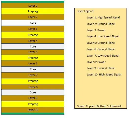
Technical Principles of Signal Integrity in High-Speed PCBs
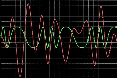
Signal integrity in high-speed PCBs hinges on maintaining consistent characteristic impedance along transmission lines to prevent reflections. Reflections occur when impedance mismatches cause portions of the signal to bounce back, distorting the waveform at the receiver. Crosstalk arises from capacitive and inductive coupling between adjacent traces, amplifying noise in dense layouts. Attenuation increases with frequency due to conductor losses, skin effect, and dielectric absorption, necessitating low-loss materials.
Dielectric properties play a pivotal role, as the dissipation factor influences signal propagation in high frequency PCB manufacturing. Stackup design must balance symmetry for warpage control and reference planes for return paths. Vias introduce discontinuities, with stub lengths affecting resonance frequencies. Engineers evaluate these through time-domain reflectometry concepts during DFM.
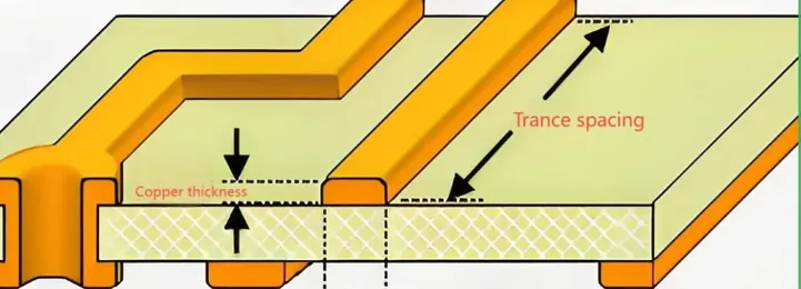
Per IPC-2221 guidelines, minimum spacing between traces mitigates crosstalk in high-speed environments. Impedance control requires precise control of trace width, thickness, and surrounding dielectric. Factory processes must achieve etch tolerances that preserve these dimensions across panels.
Key DFM Challenges in High-Speed PCB Layout
PCB layout for high speed introduces challenges like length mismatch in differential pairs, leading to skew and eye diagram closure. Routing on inner layers demands via minimization to avoid stub effects, while outer layers suit microstrips for easier impedance tuning. Ground plane splits can create return path inductance, exacerbating EMI. Manufacturing views these through panel-level effects, such as copper imbalance causing warpage.
Material selection affects DFM for controlled impedance, with resin content influencing drill smear and plating adhesion. High-frequency laminates require tighter registration to maintain layer-to-layer alignment. Aspect ratios in drilling limit via reliability under thermal cycling. Signal integrity DFM review scrutinizes these to forecast yield.
Fabrication tolerances for trace width typically tighten for high-speed designs, impacting yield if not anticipated. Plating thickness uniformity ensures low resistance in high-current paths. Solder mask application must avoid bridging high-density signals.
Practical Best Practices for Signal Integrity DFM Review
Start with stackup optimization, placing high-speed signals between ground and power planes for shielding and low inductance. Symmetric builds prevent bow and twist, critical for press-fit connectors and BGA assembly. Simulate impedance pre-layout using field solvers, then validate with test coupons on panels.
Implement length-matched routing for clocks and data pairs, using serpentine or trombone patterns judiciously to avoid resonance. Prefer broadside coupled differential pairs over edge-coupled for better manufacturability in multilayer boards. Enforce clearance rules exceeding standard values for high-speed nets.
Incorporate IPC-2141 principles for impedance test structures, embedding TDR lines in the panel border. Specify tolerances like plus or minus 10 percent, adjustable per fab capabilities. Route high-speed signals away from edges to mitigate bevel effects during routing.
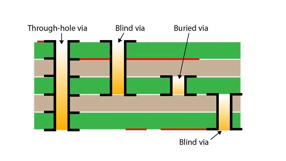
Via design favors back-drilling or blind vias to shorten stubs, though costlier; assess trade-offs in DFM. Use filled vias for thermal relief in dense areas. For high frequency PCB manufacturing, qualify materials via coupon testing for Dk stability.
Power integrity complements signal checks, ensuring clean planes without islands. Decoupling capacitors placement follows via-in-pad rules for minimal loop area. Factory DFM flags annular ring deficiencies around vias.
Troubleshooting Common Signal Integrity Issues in Manufacturing
Degraded eye diagrams often trace to impedance drift from etch undercut or over-etch. Factory feedback reveals panel bow affecting drill accuracy, misaligning high-speed vias. Crosstalk spikes post-assembly indicate insufficient spacing under solder mask.
Mitigate via resonance by modeling stub lengths below quarter-wavelength at knee frequency. Thermal expansion mismatch warps boards, stressing high-speed traces; symmetric copper distribution counters this. Per IPC-6012 qualification, verify bow and twist limits pre-shipment.
Post-DFM audits include flying probe tests on nets for continuity and shorts. Signal launches from connectors demand stub removal. Iterative reviews refine rules for future designs.
Conclusion
A comprehensive DFM review for high-speed PCBs integrates signal integrity with manufacturing feasibility, ensuring robust performance. Key practices like precise stackup, impedance control, and via optimization directly yield success in high frequency environments. Electrical engineers benefit from standard-aligned checks to preempt issues, fostering reliable production. Prioritizing these elements minimizes risks, controls costs, and elevates design quality. Future advancements will demand even tighter DFM-signal synergy for emerging speeds.
FAQs
Q1: What is high-speed PCB DFM and its role in signal integrity?
A1: High-speed PCB DFM evaluates designs for manufacturability while safeguarding signal quality at gigabit frequencies. It focuses on tolerances for traces, vias, and stackups to prevent reflections and crosstalk. Factory insights guide adjustments, ensuring controlled impedance aligns with production. This review cuts respin risks and boosts yield.
Q2: How does PCB layout for high speed impact DFM for controlled impedance?
A2: Optimal layout minimizes length variations and couples signals properly to maintain impedance. Symmetric stackups and reference planes reduce discontinuities. DFM verifies etch and drill capabilities match layout demands. Resulting boards exhibit clean eye patterns post-fabrication.
Q3: Why is signal integrity DFM review essential for high frequency PCB manufacturing?
A3: It identifies tolerance gaps that degrade signals during etching, plating, or lamination. Standards like IPC-2221 inform spacing to curb noise. Proactive review ensures low-loss propagation and EMI compliance. Manufacturers achieve higher first-pass yields.
Q4: What best practices improve DFM in high-speed designs?
A4: Embed impedance coupons, enforce tight clearances, and symmetrize copper. Prefer blind vias for critical nets and test panel warpage. Align material specs with fab limits. These steps secure signal fidelity through production.
References
IPC-2221B — Generic Standard on Printed Board Design. IPC, 2012
IPC-2141A — Design Guide for the Fabrication of High-Speed, Controlled Impedance Multilayer Printed Boards. IPC, 2009
IPC-6012E — Qualification and Performance Specification for Rigid Printed Boards. IPC, 2017