Introduction
Printed circuit boards form the backbone of modern electronics, where even minor manufacturing defects can compromise system performance and lead to field failures. In high-stakes applications like aerospace, medical devices, and telecommunications, PCB reliability directly impacts safety and operational uptime. Flying probe testing emerges as a critical tool in quality control pipelines, offering precise defect detection without the limitations of traditional fixtures. This method enhances reliability testing for PCBs by identifying issues early in the production cycle. By integrating flying probe testing defect detection into manufacturing workflows, engineers can achieve higher yields and reduce rework costs. Factories increasingly rely on this approach to meet stringent performance demands.
What Is Flying Probe Testing?
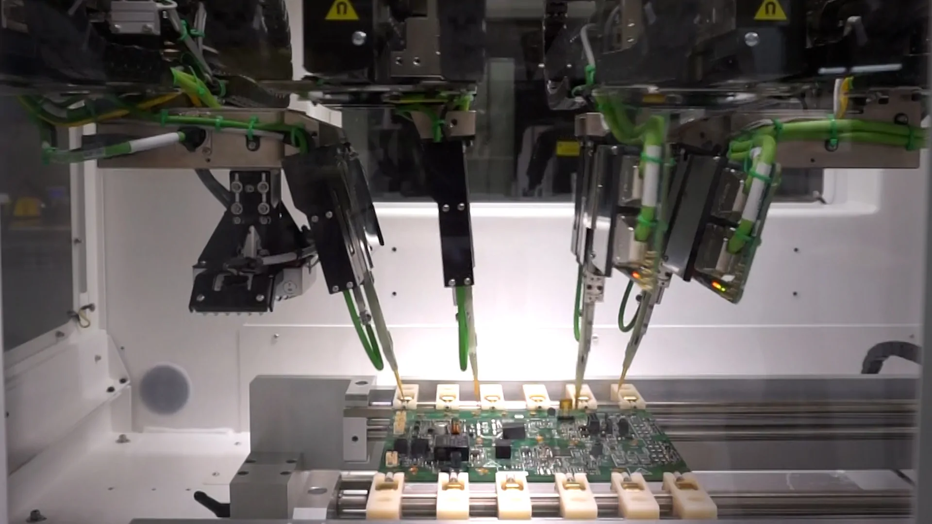
Flying probe testing, often abbreviated as FPT, is a fixtureless electrical test method for bare boards and assembled PCBs. It employs robotic arms equipped with movable probes that contact test points sequentially to measure continuity, resistance, capacitance, and other parameters. Unlike fixed-fixture systems, these probes, typically numbering four to twenty, navigate the board surface under computer control, adapting to various board sizes and layouts. This flexibility makes FPT ideal for prototypes and low-to-medium volume production. The process generates detailed test reports that pinpoint exact failure locations, aiding rapid troubleshooting. In factory settings, FPT serves as a cornerstone for FPT for quality control.
Why Flying Probe Testing Matters for PCB Manufacturing
PCB manufacturing defects, such as opens and shorts, arise from processes like etching, drilling, plating, and soldering, potentially evading visual inspections. These flaws degrade signal integrity and thermal management, leading to intermittent failures under operational stress. Flying probe testing defect detection addresses this by verifying electrical connectivity across nets, ensuring compliance with design intent. Reliability testing PCB through FPT minimizes escape rates, where defective boards reach assembly or end-use. Factories report improved first-pass yields when incorporating FPT, as it catches issues before downstream processes amplify them. This proactive stance aligns with industry goals for zero-defect production.
Common PCB Manufacturing Defects Detected by Flying Probe Testing
Open circuits top the list of PCB manufacturing defects, often resulting from incomplete etching or broken traces during handling. Flying probe testers detect these by applying voltage and checking for continuity between nodes. Shorts, caused by plating residues or solder bridges, trigger immediate alarms through low-resistance measurements. Component-related issues, like missing parts or incorrect polarity on assemblies, also fall under FPT's scope via parametric tests. Capacitance and inductance deviations signal dielectric failures or improper lamination. By systematically probing thousands of points, FPT ensures comprehensive coverage, reducing the risk of latent defects.
Technical Principles Behind Flying Probe Testing
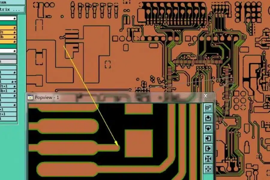
At its core, flying probe testing operates on principles of electrical measurement, starting with netlist importation from design files. Probes make physical contact at via pads, test points, and component leads, applying signals up to several volts for continuity checks. Advanced systems incorporate boundary scan for JTAG-enabled boards, expanding test depth without additional hardware. Test speed relies on probe acceleration, contact force calibration, and parallel probing to balance throughput and accuracy. Software algorithms analyze measurements against golden board signatures, flagging deviations as potential defects. This data-driven approach supports traceability in factory environments.
Factory-driven implementations tune probe pitch and z-axis force to handle fine-pitch components down to 0.3 mm. Environmental controls, like temperature-stable chambers, prevent false calls from thermal expansion. Integration with automated optical inspection precedes FPT, correlating visual and electrical data for root cause analysis. Such layered verification upholds standards like IPC-A-600 for board acceptability. Engineers appreciate the programmability, allowing custom test sequences for high-speed signals or power planes.
How Flying Probe Testing Minimizes Defects Compared to Traditional Methods
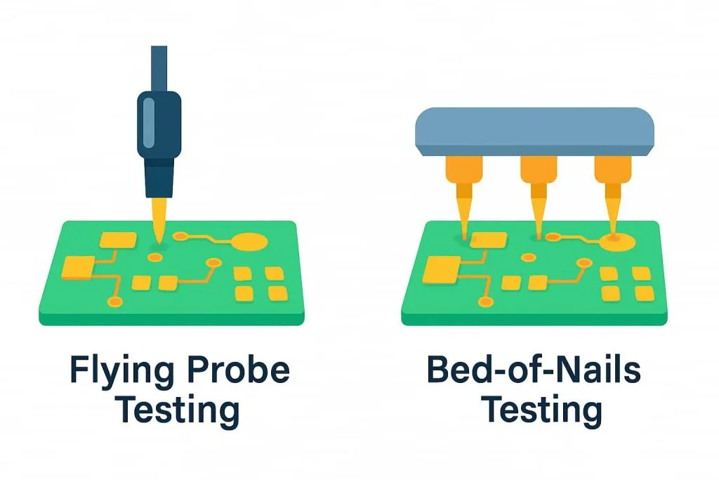
Bed-of-nails testing, or in-circuit testing, uses fixed probes for parallel measurements but demands costly custom fixtures, limiting its use for design changes. Flying probe testing bypasses this by eliminating fixtures, cutting setup time from weeks to hours. For double-sided or high-density interconnect boards, FPT accesses points inaccessible to rigid fixtures. While bed-of-nails excels in high-volume scenarios for speed, FPT offers superior flexibility for reliability testing PCB in NPI phases. Defect escape rates drop significantly with FPT's adaptive probing, as it tests 90 percent or more of nets without mechanical constraints. Factories switch to FPT for prototypes to validate designs before committing to fixtures.
Quantitative advantages include reduced false positives through dynamic contact verification and multi-frequency testing for capacitive opens. In assembly testing, FPT verifies solder joint integrity per J-STD-001 requirements without stressing components. This non-destructive nature preserves boards for further processing, unlike aggressive fixture pressure. Overall, FPT integrates seamlessly into lean manufacturing, minimizing PCB manufacturing defects across production scales.
Best Practices for FPT in Quality Control
Start by optimizing test point placement during design, allocating at least one per net per IPC-9252 guidelines for electrical testing. Collaborate with factories to import accurate netlists and golden board data, avoiding test program errors. Calibrate probes daily for consistent contact resistance below 50 milliohms, and monitor wear to maintain precision. Sequence tests from power-off continuity to powered functional checks, isolating analog and digital sections. Analyze failure maps post-run to feed back into process controls, like plating bath adjustments. Implementing these steps elevates FPT for quality control.
Incorporate statistical process control by tracking test times and yield trends, setting alerts for drifts. For multilayer boards, prioritize inner layer shorts via vectorless testing modes. Train operators on software diagnostics to expedite repairs, targeting under 5 percent rework. Pair FPT with environmental stress screening for comprehensive reliability validation. These practices, rooted in factory experience, ensure defects stay below actionable thresholds.
Conclusion
Flying probe testing stands out as a versatile solution for boosting PCB reliability amid evolving manufacturing complexities. Its ability to detect opens, shorts, and parametric faults without fixtures streamlines quality control for engineers. By embedding FPT early, factories curb PCB manufacturing defects, enhancing end-product dependability. Adopting best practices maximizes its potential, aligning with IPC standards for sustained performance. As board densities rise, FPT remains indispensable for reliable electronics production.
FAQs
Q1: What is flying probe testing defect detection, and how does it work?
A1: Flying probe testing defect detection uses movable probes to electrically verify PCB nets for opens, shorts, and component issues. Robotic arms position probes at test points, measuring resistance and capacitance against design specs. This fixtureless method suits prototypes and low volumes, providing precise fault localization via software reports. Factories leverage it for early defect isolation, improving overall yields.
Q2: How does FPT contribute to reliability testing PCB?
A2: FPT enhances reliability testing PCB by confirming electrical integrity post-manufacturing processes like etching and soldering. It identifies latent defects that visual checks miss, such as trace discontinuities or plating voids. Parametric tests ensure signal paths meet performance criteria under nominal conditions. This reduces field failure risks in critical applications. Integration with standards like IPC-A-600 verifies acceptability.
Q3: What are typical PCB manufacturing defects caught by flying probe testing?
A3: Common PCB manufacturing defects include open circuits from etching errors, shorts from residue, and wrong component values. Flying probe testing detects these through continuity and value checks at thousands of points. It also flags polarity reversals and missing parts on assemblies. Such comprehensive coverage minimizes escapes to assembly stages. Factory data shows it excels in high-density boards.
Q4: When should engineers use FPT for quality control?
A4: Use FPT for quality control in prototypes, design iterations, or low-volume runs where fixture costs outweigh benefits. It shines for double-sided, fine-pitch, or HDI boards inaccessible by bed-of-nails. Post-assembly, it validates solder joints per J-STD-001. Avoid for ultra-high volumes favoring speed. This targeted application optimizes reliability without excess tooling.
References
IPC-A-600M — Acceptability of Printed Boards. IPC, 2025
IPC-6012E — Qualification and Performance Specification for Rigid Printed Boards. IPC, 2015
IPC-9252B — Requirements for Electrical Testing of Rigid Printed Boards. IPC, 2016
J-STD-001H — Requirements for Soldered Electrical and Electronic Assemblies. IPC, 2018


