Introduction
Ball Grid Array (BGA) components present unique challenges in PCB layout due to their high pin density and compact footprint. Proper via placement BGA fanout becomes critical to ensure reliable signal routing from the dense array of solder balls to the broader board traces. Engineers must consider electrical performance, thermal management, and mechanical reliability when planning PCB fanout strategies. In high-speed designs, suboptimal via placement can lead to signal integrity issues such as crosstalk, reflections, and impedance discontinuities. HDI design techniques often incorporate microvias to address these constraints in via placement BGA components. This article explores the engineering principles and best practices for optimizing via placement in BGA fanout designs to achieve robust PCB layouts.
Understanding BGA Fanout and the Role of Via Placement
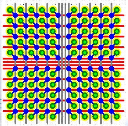
BGA fanout refers to the process of routing signals from the fine-pitch solder balls under a BGA package to accessible traces on outer or inner layers. Via placement BGA fanout determines the efficiency of this breakout, influencing routing density and layer count requirements. Traditional through-hole vias may suffice for coarser pitches, but finer pitches demand advanced strategies like via-in-pad or staggered microvias. In PCB layout, the positioning of these vias relative to BGA balls affects escape routing feasibility and overall board real estate. Poor via placement can force longer traces, increasing inductance and compromising signal integrity. Engineers prioritize via placement BGA components to balance manufacturability with performance demands.
HDI design elevates these considerations by enabling tighter via placement BGA fanout through laser-drilled microvias and sequential build-up processes. This approach supports pitches below 0.5 mm, common in modern processors and FPGAs. The choice between dogbone fanout, where vias sit adjacent to pads, and full via-in-pad depends on pitch and layer stackup. Each method carries trade-offs in terms of solder joint reliability and via reliability under thermal cycling. Standards like IPC-7095 provide guidelines for land patterns and fanout implementation to ensure consistency across designs.
Technical Principles Governing Via Placement
Via placement directly impacts electrical characteristics in BGA fanout designs. Vias introduce parasitic inductance and capacitance, which can degrade signal integrity if not minimized. For high-frequency signals, engineers position vias to maintain characteristic impedance, often staggering them across multiple rows to reduce crosstalk between adjacent signals. In PCB fanout regions, via stubs from unbackdrilled through-vias act as resonant elements, causing reflections; backdrilling mitigates this but adds cost. Optimal via placement BGA fanout aligns vias perpendicular to signal paths where possible, minimizing trace bends and associated losses.
Thermal management plays a pivotal role, as BGA packages dissipate significant heat through their balls. Vias under ground and power balls form thermal vias, channeling heat to inner planes efficiently. However, clustered thermal vias can create stress concentrations due to coefficient of thermal expansion (CTE) mismatches between copper, dielectric, and silicon. Strategic via placement BGA components distributes these thermal paths evenly, reducing localized hotspots and improving long-term reliability. IPC-2221 outlines design rules for via spacing and annular ring dimensions to prevent cracking under thermal stress.
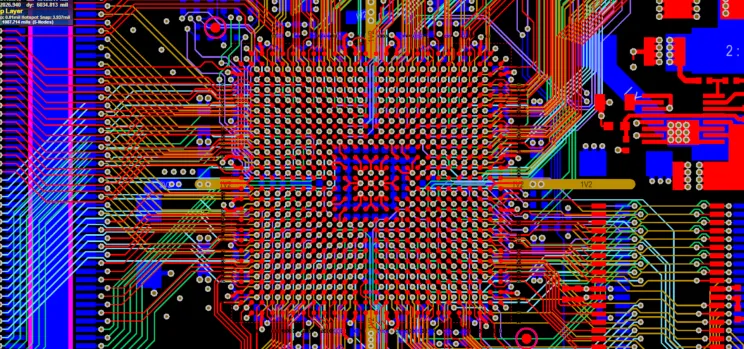
Mechanically, via placement influences board warpage and solder joint integrity during reflow. Dense via fields in HDI design can stiffen local areas, exacerbating warpage if stackup symmetry is ignored. Engineers model via placement BGA fanout using finite element analysis to predict stress distributions. Signal integrity simulations reveal how via positioning affects return paths and ground bounce. In multilayer boards, blind and buried vias enable tighter PCB fanout without penetrating the entire stackup, preserving inner layer integrity.
Related Reading: Basics of routing with BGA packages
Best Practices for Via Placement in BGA Fanout
Start with component placement to facilitate via placement BGA fanout. Position BGAs near the board center or along edges with ample routing channels, avoiding corners that limit escape options. Define fanout zones early, allocating dedicated layers for BGA breakout to prevent congestion. For pitches above 0.8 mm, use dogbone vias offset from pads at 45-degree angles to maximize density. In HDI design, transition to microvia-in-pad for finer pitches, ensuring via diameter does not exceed 20% of pad size to maintain solderability.
Impedance control demands precise via placement BGA components. Pair high-speed signals with ground vias nearby to provide low-inductance return paths, following length-matched routing. Stagger vias in a zigzag pattern across BGA rows to free up trace escape corridors on adjacent layers. Verify via-to-via spacing exceeds three times the via diameter to minimize coupling. IPC-6012DS specifies qualification criteria for HDI vias, emphasizing aspect ratios below 0.8:1 for reliable plating.
Power and ground distribution benefits from arrayed via placement BGA fanout. Dedicate peripheral balls to power planes, fanning out multiple vias per ball for low resistance. Decoupling capacitors should sit within 1 mm of signal balls, with vias directly beneath for shortest paths. In PCB layout, simulate power integrity to confirm via configurations suppress simultaneous switching noise. Thermal vias under die shadow balls enhance cooling without interfering with signal vias.
Fabrication considerations guide practical via placement. Align vias to fabrication grids for drill accuracy, and incorporate tenting over non-plated vias to prevent solder wicking. For double-sided BGA placement, coordinate via fields to avoid overlap conflicts. Post-layout DRC checks enforce minimum clearances, while DFM reviews assess via density against panel utilization.
Related Reading: Stacked Via vs. Via in Pad: Which Via Technology is Best for BGA Routing?
Common Challenges and Troubleshooting in Via Placement
Dense BGA arrays often lead to routing escapes that compromise signal integrity. Via stubs in through-hole fanouts create unwanted resonances; solutions include blind vias or backdrilling, though the latter requires precise depth control. Crosstalk arises from parallel vias in adjacent columns; mitigate by alternating signal and ground vias in a checkerboard pattern. In HDI design, microvia reliability under thermal cycling poses risks if laser drilling parameters deviate.
Warpage from asymmetric via placement BGA fanout distorts solder joints. Balance via counts across layers and use symmetric stackups. Head-in-pillow defects occur if via-in-pad processes leave residues; ensure proper solder mask expansion and reflow profiles. Troubleshooting involves X-ray inspection and cross-section analysis to correlate failures with via positioning.
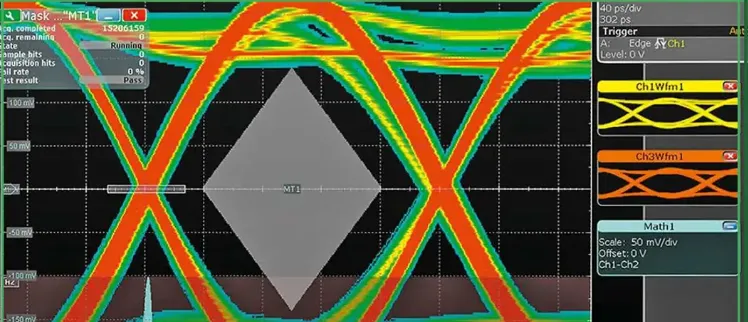
Case studies highlight these issues. A processor board with 0.4 mm pitch BGA suffered signal degradation until switching to staggered microvias, improving eye height by optimizing via placement BGA components. Another design resolved thermal hotspots by redistributing ground vias, aligning with IPC guidelines.
Conclusion
Via placement BGA fanout stands as a cornerstone of successful PCB layout for modern electronics. By adhering to structured principles in electrical, thermal, and mechanical domains, engineers achieve superior signal integrity and reliability. HDI design expands options for dense PCB fanout, but demands meticulous planning. Best practices, informed by standards like IPC-7095, IPC-2221, and IPC-6012DS, guide optimal configurations. Prioritizing via placement BGA components early minimizes redesigns and ensures high-yield production. Mastering these techniques empowers designers to tackle escalating complexity in high-performance boards.
FAQs
Q1: What factors determine optimal via placement BGA fanout?
A1: Via placement BGA fanout depends on BGA pitch, layer count, and signal speed requirements. Engineers consider impedance matching, thermal dissipation, and routing density. Staggered or via-in-pad strategies suit fine-pitch designs, while dogbone works for coarser arrays. Simulations verify performance, ensuring minimal stubs and crosstalk. HDI design enhances flexibility for complex PCB fanout.
Q2: How does via placement affect signal integrity in BGA components?
A2: Poor via placement BGA components introduces inductance and reflections, degrading eye diagrams at high frequencies. Proper positioning maintains controlled impedance and short return paths. Ground vias shield signals, reducing crosstalk. Backdrilling eliminates stubs in through-vias. PCB layout tools with SI analysis aid optimization. Consistent fanout patterns preserve waveform integrity.
Q3: What role does HDI design play in via placement BGA fanout?
A3: HDI design enables microvias for tighter via placement BGA fanout, supporting pitches under 0.5 mm. Stacked or staggered microvias free inner layers for routing. It reduces board thickness while boosting density. Sequential lamination ensures via reliability. Engineers plan stackups to align with BGA escape needs. This approach excels in high-speed PCB layout.
Q4: Why is staggering vias important in PCB fanout for BGAs?
A4: Staggering vias in PCB fanout maximizes escape trace channels across layers. It prevents congestion in dense BGA arrays, easing signal routing. This technique lowers crosstalk by separating parallel paths. Thermal vias integrate seamlessly without blocking signals. IPC guidelines recommend it for balanced performance. Proper staggering enhances overall manufacturability.
References
IPC-7095E — Design and Assembly Process Guidance for Ball Grid Arrays (BGAs). IPC, 2024
IPC-2221B — Generic Standard on Printed Board Design. IPC, 2012
IPC-6012DS — Qualification and Performance Specification for High Density Interconnect (HDI) Printed Boards. IPC, 2015


