 00:54
00:54
Via Filling
Via filling is a critical process in printed circuit board (PCB) design and manufacturing, where vias—small holes that connect different layers of a PCB—are filled with materials such as conductive epoxy, copper, or non-conductive resins. This technique enhances the board's reliability, thermal performance, and electrical integrity, making it essential for high-density interconnects and advanced electronics applications. For engineers and designers searching for via filling solutions, this tag aggregates resources that delve into the fundamentals, benefits, and implementation strategies to optimize PCB layouts. One key advantage of via filling is its ability to prevent issues like solder wicking, voids, or contamination during assembly, which can compromise board functionality. In high-frequency circuits, filled vias reduce signal loss and electromagnetic interference, while in power electronics, they improve heat dissipation by creating a more robust thermal path. Practical applications include multilayer boards for consumer devices, automotive systems, and aerospace components, where space constraints demand efficient via management. Best practices involve selecting the appropriate filling method based on board requirements—conductive fills for better conductivity or non-conductive options for insulation—while considering factors like cost, manufacturability, and compliance with standards such as IPC-4761. Professionals tackling via filling challenges can benefit from understanding common pitfalls, such as improper material selection leading to reliability failures, and how to mitigate them through design software simulations or prototyping. Articles linked under this tag offer detailed guides on techniques like screen printing, plating, or vacuum filling, along with case studies demonstrating real-world improvements in PCB performance. By exploring these resources, users gain actionable insights to refine their designs, ensuring robust and efficient electronic systems that meet modern demands.
Video Guide
-
00:54
Technical Articles

The "Black Hole" on Pads: Why Via-in-Pad Must Be Filled or Avoided

Root Causes of PCB Expansion and Shrinkage and How to Mitigate Them
Via Design Guidelines in PCB Design: Balancing Performance and Cost
Can You Place a Via on a Pad?
Which Vias Need Resin Plugging? Real Engineer Questions from Production

Should a PCB Via Be Tented or Exposed? Do Not Select the Wrong Option by Habit
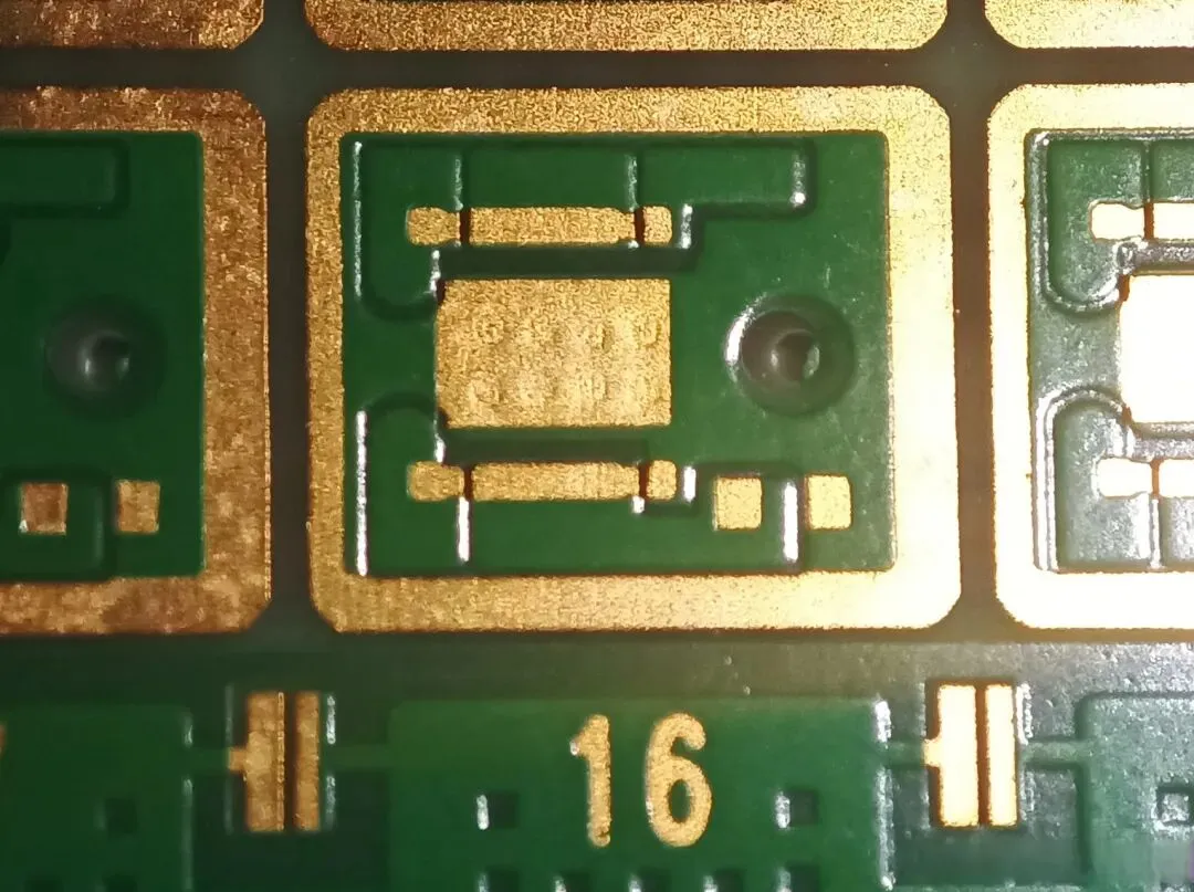
Via-in-Pad: Three Critical Manufacturing Risks and Four Valid Use Cases
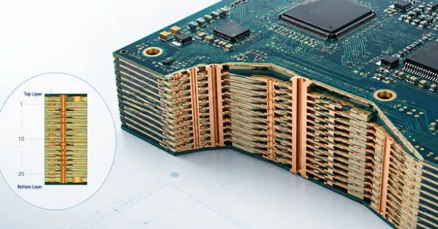
Multilayer PCB Assembly: Design and Manufacturing Considerations
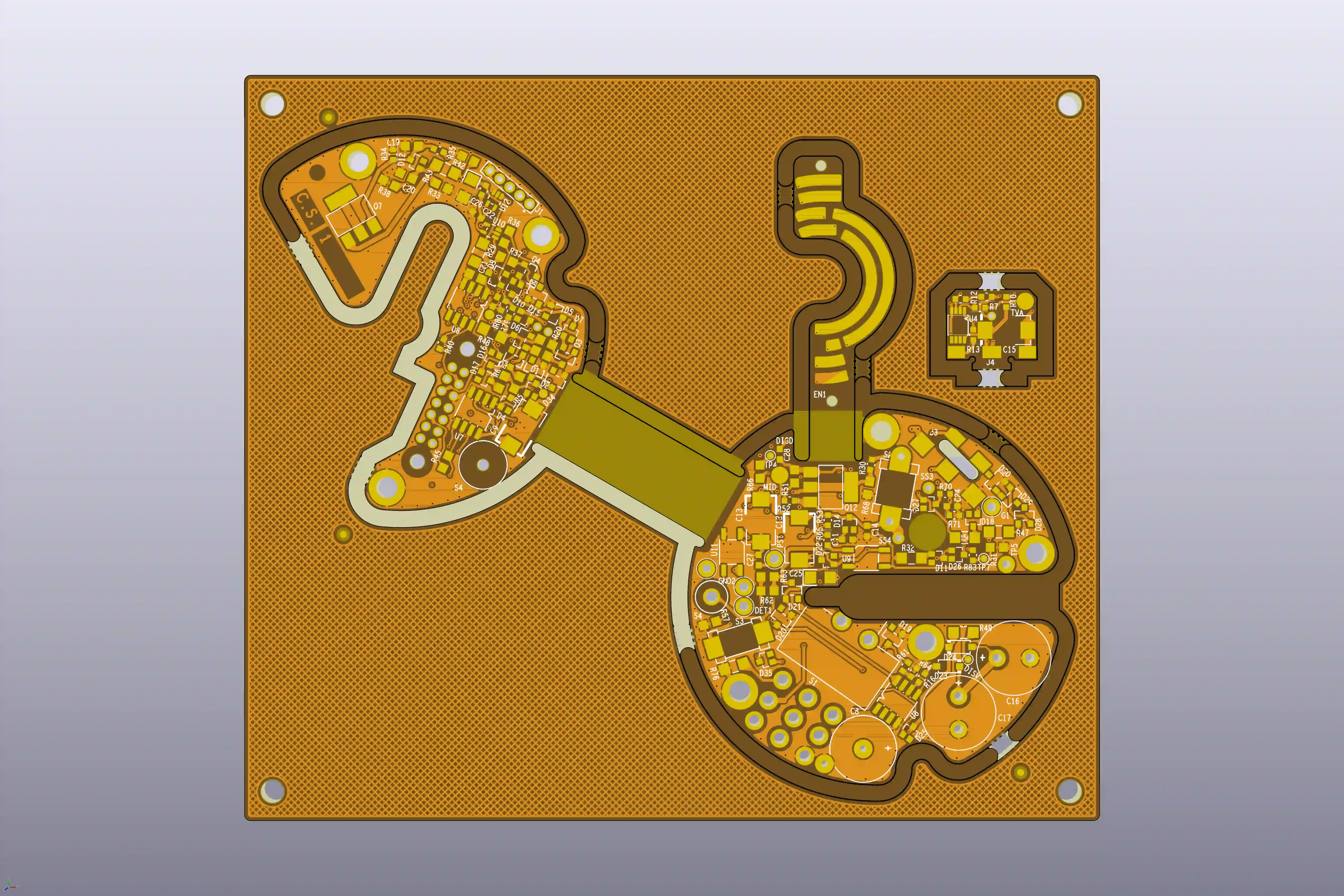
How to Avoid Edge Clearance and Via Plugging Issues in 4-Layer Rigid-Flex PCB

8-Layer FR-4 PCB with Blind Vias: Solder Mask Openings, Via Plugging and V-CUT Clearance Issues During CAM Review
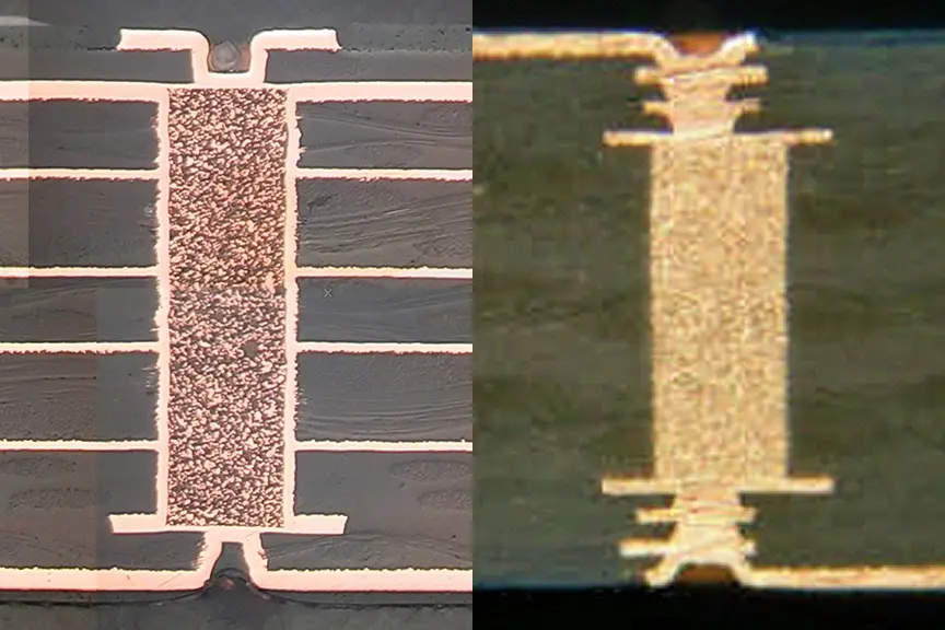
Thermal Via Filling: Choosing the Right Material for Optimal Heat Transfer
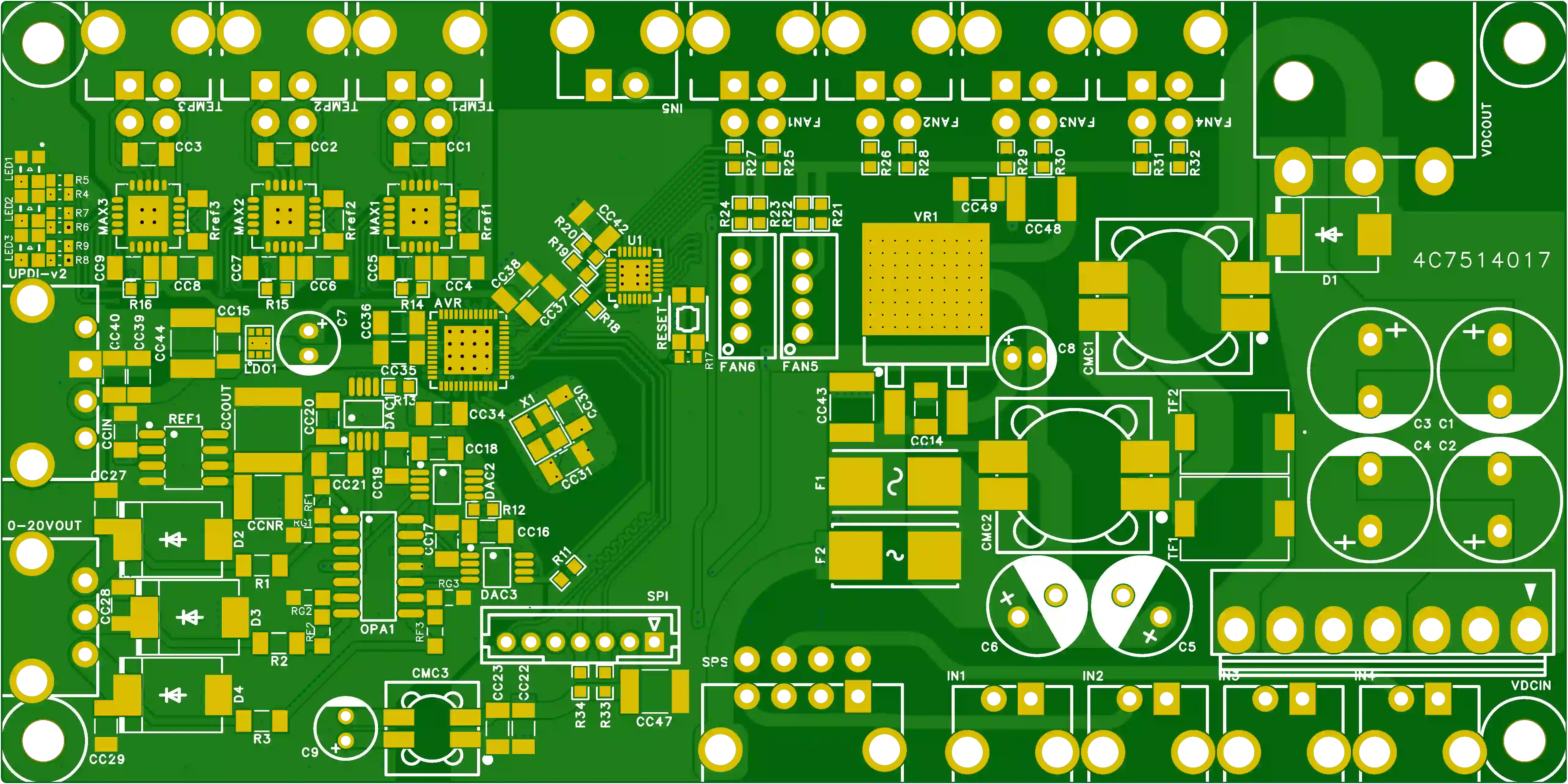
How Conflicting Via Data and Soldermask Definitions Triggered CAM Review in a 4-Layer HDI PCB
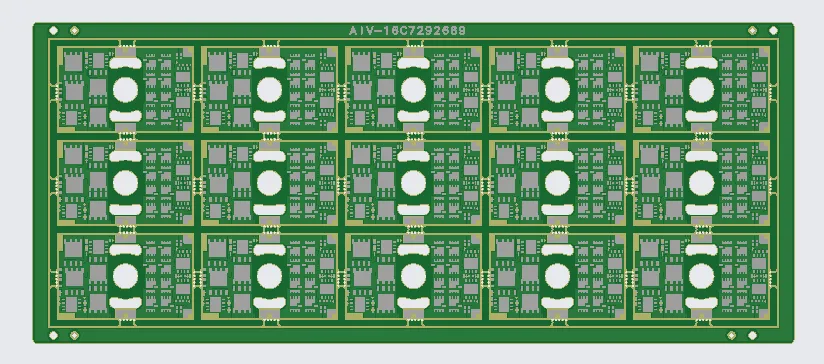
16 Layer PCB CAM Review: HDI Stackup Optimization and Resin Plugging for Reliable Fabrication
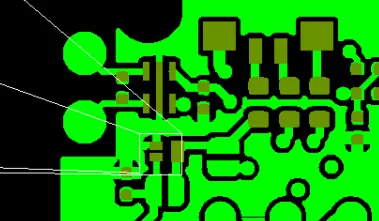
Resin Filled Via & Blind Via Issues in 6-Layer 2nd Order HDI PCB CAM Review
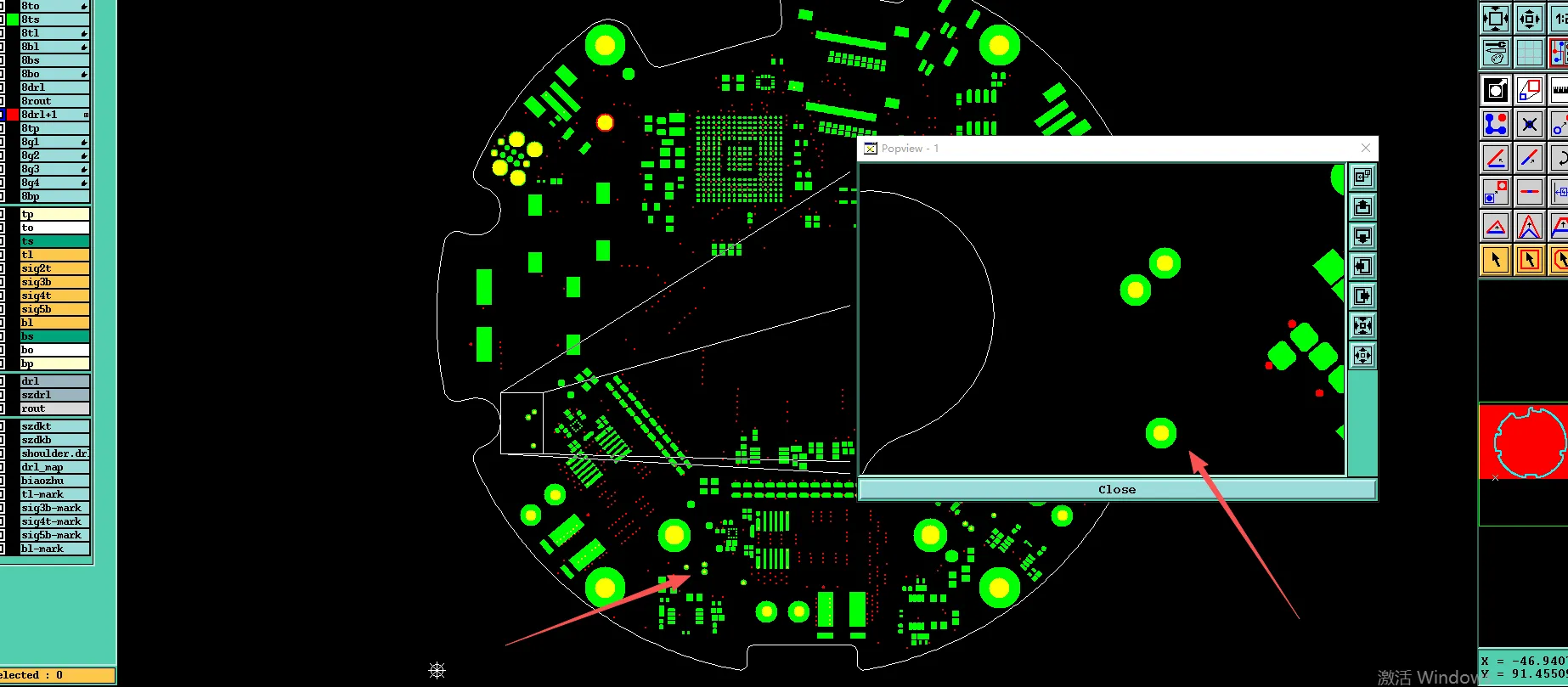
Avoiding DFM Delays: A Guide to PCB Resin Filled Via Design
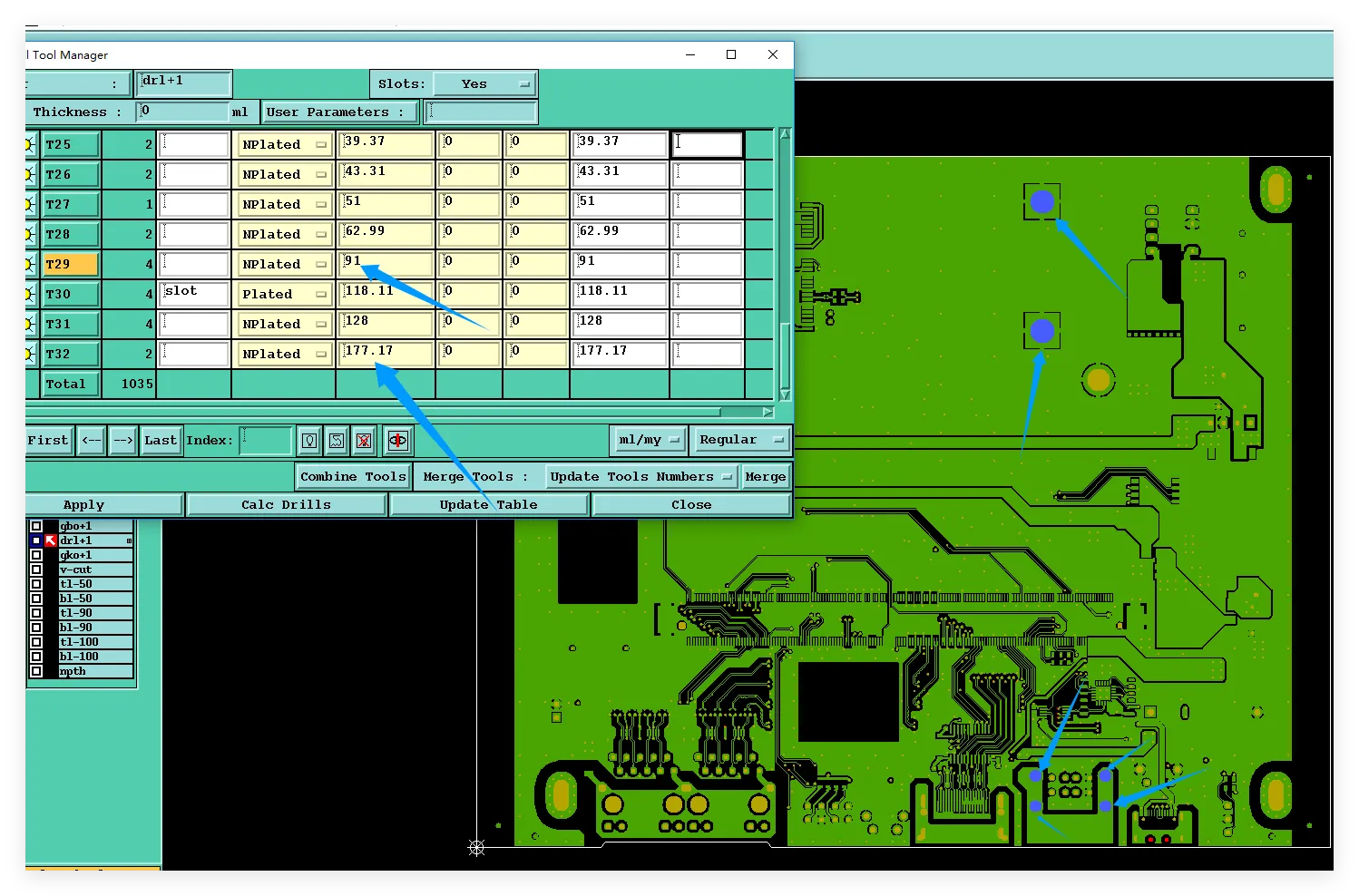
PCB Via-in-Pad Design Rules: Avoiding SMT Assembly Voids
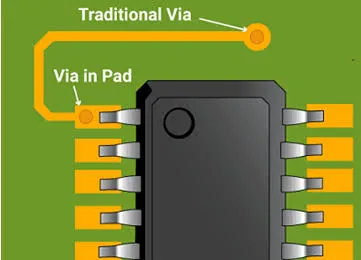
Via-in-Pad vs Traditional Via Routing for HDI PCB
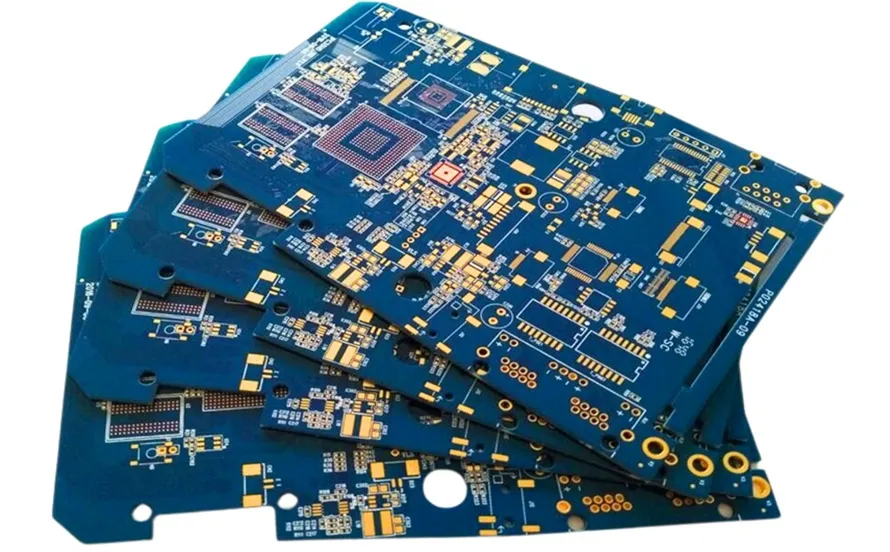
Common Via-in-Pad Design Mistakes in HDI PCB
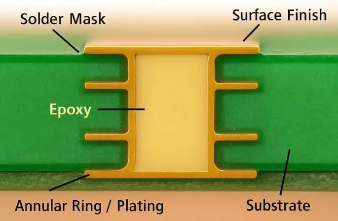
Resin Filled Via vs Copper Filled Via HDI: What Is the Difference?