










In a recent 4-layer FR4 order for a compact electronics module, our DFM review identified several manufacturability concerns that could have compromised yield and long-term reliability if left unaddressed. The board measured just 53.87 x 24.07 mm with 1.0 mm finished thickness, using 0.5 oz outer copper and 1 oz inner layers, ENIG surface finish, and blue solder mask. With only 10 pieces required, precision in every process step was critical to avoid scrap and ensure consistent performance.
From a DFM perspective, even straightforward-looking designs on thin, small-form-factor boards can harbor hidden risks related to copper clearance, via plugging consistency, impedance control, and feature interactions. Early engineering clarification prevented potential issues such as exposed copper, incomplete plugging, and signal integrity variations before production began.
Why This Compact 4-Layer Design Needed Detailed DFM Scrutiny
The PCB ( #FR4-20260116-011 ) featured standard FR-4 TG130 material, 0.25 mm hole size, and mechanical forming. Key process elements included resin plugging for certain vias, impedance requirements on specific traces, and silkscreen markings on openings. While the design appeared manufacturable at first glance, the combination of small overall dimensions, mixed copper weights, and specific via treatments raised flags for manufacturing stability.
Our CAM engineering team flagged potential risks around copper-to-hole clearances, single-sided versus double-sided solder mask openings, and the interaction between plugged vias and silkscreen. These are common areas where minor oversights can lead to significant downstream problems during lamination, drilling, plating, or assembly. The goal was to confirm design intent and align processes to maintain high yield even on a short 11-day delivery schedule.
Critical Manufacturability Risks Identified During Review
The top concerns centered on three areas: via plugging consistency with mixed opening types, copper clearance near non-plated holes, and precise impedance control boundaries. These issues stood out because they directly impact reliability features like via integrity and surface protection.
First, the requirement for resin plugging needed clarification on holes with single-sided solder mask windows and nearby silkscreen character frames. Second, certain non-plated holes were positioned very close to copper pours, risking exposed copper after processing. Third, the stackup and impedance control zones required confirmation to ensure controlled traces (marked in design highlights) would meet targets without affecting pads.
| Risk Area | Design Feature | Potential Impact if Unaddressed |
|---|---|---|
| Via Plugging | Single-sided openings with silkscreen | Incomplete fill, resin overflow, or cosmetic defects |
| Copper Clearance | Non-plated holes near copper | Exposed copper, shorts, or corrosion risk |
| Impedance Control | Yellow trace zones only | Inconsistent signal performance |
Additionally, clarification was needed on the purpose of specific GKO layer elements and double-sided openings on four particular holes marked with silkscreen identifiers.
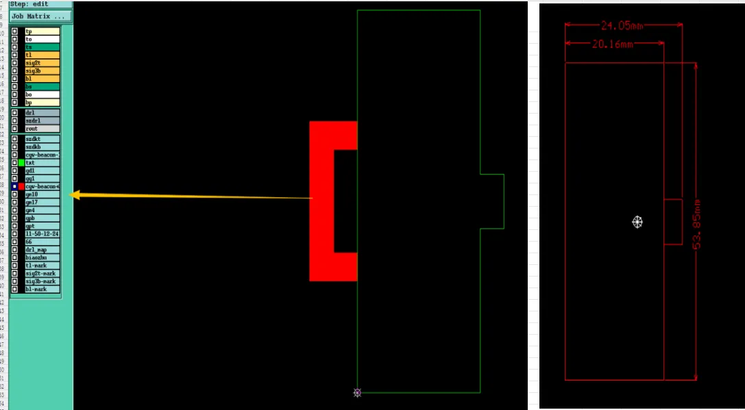
Figure 1: specific GKO layer elements
Potential Failure Scenarios Avoided Through Proactive Review
Had the design proceeded without these engineering questions, several realistic failure modes could have emerged. For resin-plugged vias with single-sided windows, incomplete or inconsistent plugging might have allowed flux or contaminants to enter during assembly, leading to via cracking under thermal stress or long-term reliability failures. In severe cases, this could result in open circuits or intermittent signal issues after deployment.
The close proximity of non-plated holes to copper features posed a high risk of exposed copper after etching and solder mask application. Ignoring this could cause poor solderability in adjacent areas, increased corrosion susceptibility in humid environments, or even unintended electrical shorts during assembly. According to IPC-A-600 acceptability criteria, exposed copper in such locations often leads to rejectable conditions that compromise both cosmetic and functional quality.
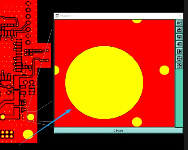
Figure 2: the NPTH is too close to the copper layer
Impedance control limited to specific traces without clear boundary confirmation could have produced inconsistent dielectric performance across the board, resulting in signal reflections or timing issues in the end product. On a 1.0 mm 4-layer stackup with mixed copper weights, any misalignment in lamination or trace compensation might exacerbate warpage risks, though the small board size helped mitigate overall panel-level distortion.

Figure 3: impedance control applies only to the yellow-colored lines
| Scenario | Root Cause | Likely Consequence |
|---|---|---|
| Exposed Copper | Insufficient clearance | Corrosion, shorts, assembly defects |
| Plugging Failure | Unclear single-sided windows | Contamination, via reliability drop |
DFM Recommendations and Engineering Resolutions
Our team recommended confirming resin plugging requirements specifically for holes with single-sided openings and silkscreen proximity to ensure proper mask and fill processes. We suggested verifying whether full plugging or alternative treatments were needed to maintain surface planarity and prevent resin bleed onto marked areas.
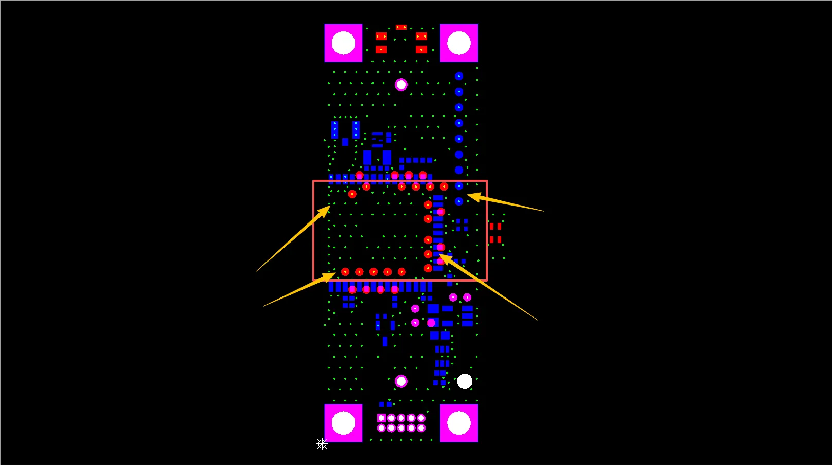
Figure 4: confirming resin plugging requirements
For the clearance concern, we proposed adjusting or confirming minimum spacing around non-plated holes to guarantee full solder mask coverage and copper protection post-processing. This aligns with practical manufacturing tolerances for ENIG finish and helps avoid exposed base material that could lead to reliability degradation.
On impedance, we requested stackup confirmation and agreement that control would apply only to designated traces. The provided calculations were reviewed against our standard FR-4 dielectric models to ensure feasibility. Double-sided openings on the four marked holes were verified for process compatibility.
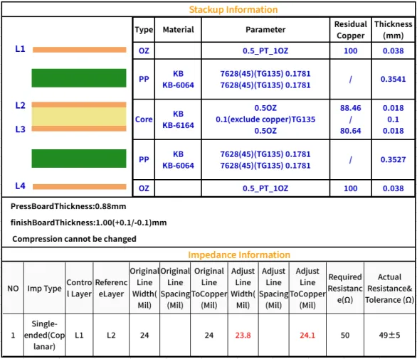
Figure 5: final stack-up
The GKO layer elements were clarified as part of the customer's design for specific manufacturing or testing purposes, allowing our CAM team to preserve them accurately. All recommendations were presented with visual references from the gerber data, enabling quick customer response and alignment.
| Recommendation | Technical Justification | Expected Benefit |
|---|---|---|
| Plugging Clarification | Ensure uniform fill on mixed openings | Improved via reliability and surface quality |
| Clearance Adjustment | Prevent post-etch exposure per IPC guidelines | Reduced corrosion and short risk |
| Impedance Confirmation | Align stackup with controlled zones | Consistent electrical performance |
Client collaboration was straightforward — responses to the EQs allowed rapid updates, demonstrating the value of clear communication during the engineering phase. Production proceeded only after all points were resolved, maintaining the original schedule.
The Value of Early DFM Engagement for Reliability
This case illustrates how proactive DFM review shifts potential problems from the production floor to the engineering stage. By addressing plugging details, clearance risks, and impedance boundaries upfront, we protected yield on a small 10-piece run and supported the board's intended reliability in its end application.
Designers benefit when manufacturers ask targeted questions rather than assuming intent. These preventive steps reduce scrap, minimize assembly issues, and contribute to more stable long-term product performance. We encourage engaging DFM expertise as early as possible in the design cycle, particularly for boards with via treatments, mixed features, or tight tolerances.
FAQ
Q1: Why is confirmation needed for resin plugging on holes with single-sided solder mask openings?
A1: Single-sided openings can lead to uneven resin fill or overflow onto silkscreen areas if not properly specified. Without clarification, incomplete plugging risks contamination paths or surface irregularities that affect reliability and assembly. Confirming the exact requirement allows the process to match design intent and prevents via-related failures.
Q2: What risks arise when non-plated holes are too close to copper features?
A2: Insufficient clearance can result in exposed copper after etching or plating processes, leading to corrosion, solder bridging, or electrical shorts. In field use, this may cause premature failures. DFM review ensures adequate spacing to maintain full coverage and long-term protection.
Q3: How does limiting impedance control to specific traces affect manufacturing?
A3: Clear zone definitions prevent over-control on non-critical areas like pads, which could otherwise complicate etching or compensation. Proper confirmation ensures the stackup delivers consistent impedance where needed while respecting manufacturing tolerances for the overall board.
Q4: Why review GKO layers and double-sided openings during CAM?
A4: These features influence mask application, drilling, or testing. Misunderstanding their purpose can lead to incorrect processing and defects. Clarification preserves intended functionality and avoids unnecessary rework or yield loss.
Q5: What makes copper balance and clearance critical even on small 4-layer boards?
A5: Uneven distribution or tight clearances can still cause local etching variations, solder mask issues, or thermal stress points. Addressing them early prevents defects that impact both immediate production yield and field reliability.
Q6: How does DFM review contribute to better PCB yield?
A6: By identifying and resolving potential issues like plugging inconsistencies or clearance violations before fabrication, DFM reduces scrap rates, ensures process compatibility, and supports consistent quality across the production run.






