










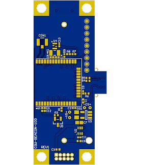
PCB Specifications
| Parameter | Value | Parameter | Value |
|---|---|---|---|
| PCB Type | FR4 PCB | Quantity | 10 pcs |
| Layers | 4 Layers | Board Type | Single PCB |
| Dimensions | 53.87 x 24.07 mm | Copper Weight | 1oz |
| Thickness | 1 mm | Min Track / Spacing | 6/6mil↑ |
| Surface Finish | ENIG (Immersion Gold) | Min Hole Size | 0.25mm |
| Solder Mask | Blue | Silkscreen | White |
| Stack-up | Custom | Impedance Control | Yes |
Manufacturing Timeline
Logistics Information
Key Manufacturing Processes
Manufacturing Summary
This compact 4-layer FR-4 board measured 53.87 × 24.07 mm with 0.5 oz inner and 1 oz outer copper and a 1.0 mm finished thickness using KB-6160 TG130 material. Produced in a quantity of 10 pieces as single boards, the design featured 6 mil line/space, ENIG surface finish, resin plugging, and impedance control. The thin copper weights and small form factor required careful stackup optimization to meet both mechanical and electrical targets.
DFM review addressed several layout specifics. Resin plugging confirmation was needed for vias with single-side openings and nearby character frames. Non-plated holes near copper features were adjusted to prevent edge exposure after routing. Impedance control was applied selectively to designated traces while excluding pads per customer guidance. Stackup calculations were verified against the target board thickness and impedance requirements. GKO layer elements and double-sided via openings received clarification before release. Impedance stackup verification ensured the final configuration balanced dielectric thicknesses and copper weights for consistent performance.
All boards passed 100% flying probe testing successfully within the 11-day schedule. The final parts maintained good registration and surface quality, supporting reliable signal integrity and assembly for this low-volume order.
Explore More PCB Manufacturing Resources
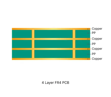
4 Layer FR4 PCB Manufacturing Insights
Standard multilayer solution offering practical routing density and controlled impedance for industrial and consumer electronics.

Multilayer FR4 PCB Engineering Queries Explained: Causes, Risks and Solutions
In-depth guide to the most frequent Engineering Queries (EQ) and DFM issues in Multilayer FR4 PCB (4/6/8+ layers) production. Real factory insights on stack-up confirmation, impedance control, copper balance, inner layer design, via treatment, registration, and practical prevention strategies.
Real Production Records
| Order ID | PCB Type | Layers | Dimensions | Solder Mask | Surface Finish | Quantity | Action |
|---|---|---|---|---|---|---|---|
| FR4-20260918-083 | FR4 PCB | 4 | 98 x 25 | Green | HASL Lead Free | 10 | View detail |
| FR4-20260918-033 | FR4 PCB | 6 | 55 x 41.7 | Green | ENIG (Immersion Gold) | 5 | View detail |
| FR4-20260912-059 | FR4 PCB | 2 | 275 x 193.7 | Green | ENIG (Immersion Gold) | 100 | View detail |


