










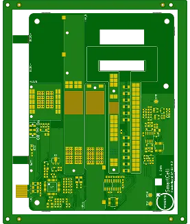
PCB Specifications
| Parameter | Value | Parameter | Value |
|---|---|---|---|
| PCB Type | FR4 PCB | Quantity | 20 pcs |
| Layers | 4 Layers | Board Type | Single PCB |
| Dimensions | 119 x 98 mm | Copper Weight | 2oz |
| Thickness | 1.2 mm | Min Track / Spacing | 6/6mil↑ |
| Surface Finish | ENIG (Immersion Gold) | Min Hole Size | 0.3mm↑ |
| Solder Mask | Green | Silkscreen | White |
| Stack-up | Default | Impedance Control | No |
Manufacturing Timeline
Logistics Information
Key Manufacturing Processes
Manufacturing Summary
This 4-layer FR-4 board measured 119 × 98 mm with 1 oz inner and 2 oz outer copper and a 1.2 mm finished thickness using KB-6165F TG150 material. Produced in a quantity of 20 pieces as single boards, the design featured 6 mil line/space, ENIG surface finish, and blind vias. Finished board thickness markings were added per customer request. The controlled depth milling requirement to expose inner layer pads presented the primary manufacturing consideration.
DFM review verified the stackup for the tight 1.2 ± 0.12 mm tolerance. Controlled depth milling was set to approximately 0.78 ± 0.1 mm to precisely reveal L2 and L3 pads, followed by surface treatment on the exposed areas. Production and panelization files were confirmed after iterative updates. Stackup and milling parameters were adjusted to maintain structural integrity while achieving the required exposure without damaging adjacent layers. Controlled depth milling registration ensured accurate depth control and clean pad exposure across the batch.
All boards completed 100% flying probe testing successfully within the 27-day schedule. The final parts met dimensional, electrical, and visual specifications, with the depth-milled features providing the intended inner layer access while preserving overall board reliability.
Explore More PCB Manufacturing Resources
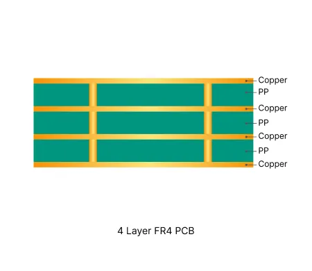
4 Layer FR4 PCB Manufacturing Insights
Standard multilayer solution offering practical routing density and controlled impedance for industrial and consumer electronics.

How to Avoid Common Engineering Queries in Multilayer FR4 PCB Design
Real multilayer FR4 PCB CAM review cases covering stack-up confirmation, impedance control, copper balance, via tenting, and edge clearance EQs. Discover practical DFM best practices for 4-layer and higher boards to reduce engineering queries, prevent warpage, and improve first-pass yield.
Real Production Records
| Order ID | PCB Type | Layers | Dimensions | Solder Mask | Surface Finish | Quantity | Action |
|---|---|---|---|---|---|---|---|
| FR4-20260918-083 | FR4 PCB | 4 | 98 x 25 | Green | HASL Lead Free | 10 | View detail |
| FR4-20260918-033 | FR4 PCB | 6 | 55 x 41.7 | Green | ENIG (Immersion Gold) | 5 | View detail |
| FR4-20260912-059 | FR4 PCB | 2 | 275 x 193.7 | Green | ENIG (Immersion Gold) | 100 | View detail |


